Full Adder
A full adder is a digital circuit that performs addition on three input bits and produces a sum and a carry output. It is a fundamental building block in digital arithmetic circuits and is used in the design of processors and other computational devices. The full adder is capable of adding two binary numbers along with a carry input from a previous addition.
7 Key excerpts on "Full Adder"
 eBook - ePub
- M. Michael Vai(Author)
- 2017(Publication Date)
- CRC Press(Publisher)
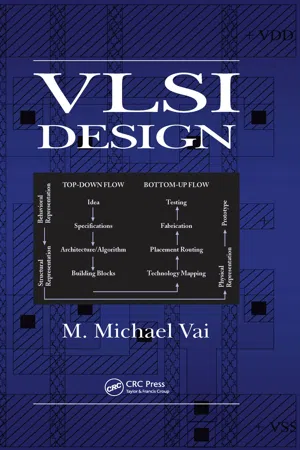
...The basic element available for building an adder is a Full Adder. Fig. 7.1 shows that a one-bit Full Adder accepts two 1-bit operands (a i, b i) and one carry-in bit (c i −1) and produces a result consisting of 1 sum bit (s i) and 1 carry-out bit (c i). An alternative view of the one-bit Full Adder is that it accepts three 1-bit operands and produces a two-bit sum. Fig. 7.1 One-bit full-adder. A number of one-bit Full Adders can be cascaded to form a ripple-carry adder (see Fig. 7.2). The ripple-carry adder is extremely modular since it contains only one-bit Full Adders. The structure is also very regular. All Full Adders in the ripple-carry adder are connected to their neighbors in the same way. The interconnections within the ripple-carry adder are limited to between neighboring Full Adders. The Full Adder cell can be laid out to accept a carry-in bit (c i −1) from its right edge and produces a carry-out bit (c i) at its left edge. This layout will facilitate the use of tessellation to the design of a ripple-carry adder. Fig. 7.3 illustrates that when two Full Adder cells are placed side by side, their power rails (V DD and V SS) as well as their carry paths are connected. It is also quite simple to expand a ripple-carry adder. An n -bit ripple-carry adder can be expanded to accept (n + m)-bit operands by incorporating m additional full-adder cells. Fig. 7.2 Ripple carry adder. Fig. 7.3 Full Adder tessellation. A ripple-carry adder has a computation time that is proportional to the number of bits in its operands. The wider the operands, the longer does it take the ripple-carry adder to complete its addition. Whether this presents a limitation or not on the use of a ripple-carry adder naturally depends on the application on hand...
 eBook - ePub
Microprocessor and Microcontroller Interview Questions:: A complete question bank with real-time examples
A complete question bank with real-time examples
- Anita Gehlot(Author)
- 2020(Publication Date)
- BPB Publications(Publisher)
...A half adder performs the addition of two inputs, and it produces two outputs namely sum and carry. In the truth table, A and B is termed as inputs while the outputs sum and carry are named as S and C respectively. Block diagram: Circuit diagram: Truth table: Input Output A B Sum Carry 0 0 0 0 0 1 1 0 1 0 1 0 1 1 1 1 Boolean expression: Sum = A’B + AB’ Carry = AB Full Adder Full Adder performs addition operation when the augend and addend number contain more than 2 digits. The carry obtained from the addition of 2 bits is added to the next higher pair of significant bits. Here, the addition operation involves 3 bits, which are augend bit, addend bit and carry bit respectively. The outputs of the Full Adder are also referred as sum and carry. Block diagram: Circuit diagram: Truth Table: Input Output A B X S C 0 0 0 0 0 0 0 1 1 0 0 1 0 1 0 0 1 1 0 1 1 0 0 1 0 1 0 1 0 1 1 1 0 0 1 1 1 1 1 1 Encoder and Decoder Encoder An encoder is a combinational circuit that converts binary information in the form of a 2N input lines. into N output lines, which represent N bit code for the input. For simple encoders, it is assumed that only one input line is active at a time. Decoder Decoders are digital ICs which are used for decoding. In other words, the decoders decrypt or obtain the actual data from the received code, i.e. convert the binary input at its input to a form, which is reflected at its output. It consists of n input lines and 2^n output lines. A decoder can be used to obtain the required data from the code or can also be used for obtaining the parallel data from the serial data received. Multiplexer and Demultiplexer Multiplexer Multiplexer means many into one. A multiplexer is a circuit used to select and route any one of the several input signals to a signal output. A simple example of a non-electronic circuit of a multiplexer is a single pole multi position switch. Multi-position switches are widely used in many electronics circuits...
 eBook - ePub
- Brian Holdsworth, Clive Woods(Authors)
- 2002(Publication Date)
- Newnes(Publisher)
...In the sum shown in Figure 12.1(a), a carry is generated in the least significant column and is then added in at the second stage where a further carry is generated. The carry has rippled through two stages of the addition. Carry ripple, through many stages, in adder circuits generates unacceptable delays, and methods are now available to eliminate this problem. Figure 12.1 (a) Binary addition. The half adder is used for adding together the two least significant bits (dotted) (b) The addition of the four possible combinations of two binary digits A and B (with a carry to the next most significant stage of addition) (c) Truth table for the half adder (d) NAND implementation of the half adder (e) NOR implementation of the half adder The additions shown in Figure 12.1(b) are tabulated in the truth table (see Figure 12.1(c)). The columns headed A and B display every combination of the two binary digits to be added, while the third and fourth columns are the corresponding tabulations of the sum S and carry C, respectively. The Boolean equations for the sum and carry read directly from the truth table are: The implementation of the sum and carry functions using NAND and NOR logic is illustrated in Figure 12.1(d) and 12.1(e). 12.3 The Full Adder When adding any pair of digits other than the least two significant digits a Full Adder is required. The Full Adder circuit has three inputs and two outputs which are shown in the block diagram (see Figure 12.2(a))...
 eBook - ePub
- John Stonham(Author)
- 2017(Publication Date)
- CRC Press(Publisher)
...Design of arithmetic processors 7 Objectives □ To design logic circuits for arithmetic. □ To examine ways of increasing the speed of arithmetic units. □ To develop a programmable arithmetic unit capable of performing a number of arithmetic calculations. □ To introduce the concept of a programming language. An important application of logic is in an arithmetic unit. Such a device must be capable of being reconfigured to enable it to carry out a range of numerical operations. This ability to carry out many different operations, depending on the problem needing to be solved, leads to the concept of a programmable system – a computer. The main components of an arithmetic unit will be developed in this chapter and a simple system controller will be specified. An elementary programming language for operating this system will be developed. Ripple-through-carry addition The addition of two binary inputs has already been considered in Chapter 3. The combinational logic designs for a Full Adder circuit which accepts input bits A and B and generates the sum A plus B, plus any carry-in together with the resulting carry-out, are given in Fig. 3.9. This Full Adder circuit can only provide the sum of two single-bit inputs – a very limited device. To extend the resolution of the adder, the cells can be cascaded where each cell receives one corresponding bit from each of the two input numbers to be added together and the carry is propagated from cell to cell as shown in Fig. 7.1. See page 59. Any system must be designed for the worst case – it could happen in practice. Such a system is known as a ripple-through-carry adder because in the worst case each cell produces a carry and each successive cell cannot generate the correct summation until the previous, i.e. lesser significant cell, has generated its carry output. Consider a ripple-through-carry adder of 8-bits resolution, performing the addition A + B where A = 127 10 and B = 1 10 Fig...
 eBook - ePub
Digital Design
Basic Concepts and Principles
- Mohammad A. Karim, Xinghao Chen(Authors)
- 2017(Publication Date)
- CRC Press(Publisher)
...Synchronous Arithmetic 10.1 Introduction A number of important combinatorial as well as sequential subsystems design such as those of multibit adders, registers, counters, decoders, multiplexers, and comparators have already been explored. We have also introduced register transfer language (RTL) and shown how it can be used to assemble various combinatorial and sequential modules to form more complex digital systems. One of our goals is to comprehend sufficiently how complex digital systems work in order to be able to design and assemble functional components. Digital computers, in particular, often involve multiple transfers of multibit data between registers and at appropriate times subject these data sets to multibit arithmetic and or logic operations. The register transfers are often interlinked with the control unit that coordinates data transfers as well as executes arithmetic and /or logic operations in a specific order. The RTL algorithm that describes the sequence of operations provides enough clues for the design of data as well as the corresponding control unit. This chapter introduces the RTL algorithms necessary for implementing primarily sequential arithmetic operations. 10.2 Serial Adder/Subtractor We introduced earlier the concept of binary serial addition and in connection to that operation had discussed a sequential logic circuit as shown in. In serial addition, we start with the LSB; one bit of addend and one bit of augend are shifted right into a single-bit FA. The resultant sum bit is stored then at the MSB of either the addend or augend register. Coincident with the clock, the carry-out of the current add operation is fed back as carry-in to the same FA; the other two FA inputs will include the next pair of shifted addend and augend bits. This shift and add operations cycle is repeated until all bits of the addend and augend have been processed...
 eBook - ePub
- J. Crowe, Barrie Hayes-Gill(Authors)
- 1998(Publication Date)
- Butterworth-Heinemann(Publisher)
...This is exactly what the Full Adder, described earlier in Section 4.1.5, does. Consequently by joining four Full Adders together, with the carry-out from one adder connected to the carry-in of the next, a four-bit adder can be produced. This is shown in Fig. 4.15. Fig. 4.15 A four-bit ripple carry adder constructed from four Full Adders This implementation is called a parallel adder because all of the inputs are entered into the circuit at the same time (i.e. in parallel, as opposed to serially which means one bit entered after another). The name ripple carry adder arises because of the way the carry signal is passed along, or ripples, from one Full Adder to the next. This is in fact the main disadvantage of the circuit because the output, S 3, may depend upon a carry out which has rippled along, through the second and third adders, after being generated from the addition of the first two bits. Consequently the outputs from the ripple carry adder cannot be guaranteed stable until enough time has elapsed 3 to ensure that a carry, if generated, has propagated right through the circuit. This rippling limits the operational speed of the circuit which is dependent upon the number of gates the carry signal has to pass through. Since each Full Adder is a two-level circuit, the full four-bit ripple carry adder is an eight-level implementation. So after applying the inputs to the adder, the correct output cannot be guaranteed to appear until a time equal to eight propagation delays of the gates being used has elapsed. The advantage of the circuit is that as each Full Adder is composed of five gates 4 then only 20 gates are needed. The ripple carry, or parallel adder, is therefore a practical solution to the production of a four-bit adder...

- Ed Lipiansky(Author)
- 2012(Publication Date)
- Wiley-IEEE Press(Publisher)
...It can be built with FA’s or other type of logic. Finally Figure 8.22 c depicts the most compact form of all three of representing a 4 -bit binary adder. These types of symbols are very convenient to use when we deal computer architecture issues and micro controllers in general. Figure 8.22 (a) 4 -bit binary adders built with FA ; (b) compact form of a 4 -bit binary adder; (c) an even more compact form of a 4 -bit binary adder. 8.5.2 Notes about Full-Adder Timing Let us assume a FA just like the one depicted in Figure 8.21. When all inputs are applied to the FA’s simultaneously, there are two delays; one of them is the delay that it takes for output S before to settle down to a valid value. The other delay is the time that it takes the C out output to settle down and become valid. Since it takes some longer time for C out to settle to a valid value, C out practically becomes the gating factor or the slow timing path, for the complete sum to be ready. The complete sum refers to the availability of valid values for S and for C out. Since S is valid a little earlier that C out, we then say that C out is the long path in the sum. Now let us call this longer delay the full-adder delay, which at the moment we do not care about its absolute value in nano-seconds. When we build a 4 -bit adder like the one shown in Figure 8.22 a note that we now call the complete sum the availability of all outputs of the 4-bit adder, i.e. valid S 3, S 2, S 1, S 0, and C 4, which is also the overall carry out of the adder. From the 4- bit adder point of view we do not care (to a point) about the availability of valid internal carries that propagate through the adder. We do care about them from the perspective that the longer it takes for those carries to propagate through the internal logic the longer it will take to obtain the complete sum. For the 4 -bit adder of Figure 8.22 a, implemented with full-adders, the overall adding time is four full-adder delays...