![]() NANOMATERIALS AND NANODEVICES
NANOMATERIALS AND NANODEVICES![]()
III-V COMPOUND SEMICONDUCTOR NANOWIRES FOR
OPTOELECTRONIC DEVICE APPLICATIONS
Q. GAO, H. J. JOYCE, S. PAIMAN, J. H. KANG, H. H. TAN
Department of Electronic Materials Engineering, Research School of Physics and Engineering,
The Australian National University, Canberra, ACT 0200, Australia
[email protected] Y. KIM
Department of Physics, Dong-A University, Busan 604-714, Korea
L. M. SMITH, H. E. JACKSON
Department of Physics, University of Cincinnati, Cincinnati, Ohio 45221-0011, USA
J. M. YARRISON-RICE
Department of Physics, Miami University, Oxford, Ohio 45056, USA
J. ZOU
School of Engineering and Centre for Microscopy and Microanalysis, The University of Queensland,
Brisbane, QLD 4072, Australia
C. JAGADISH
Department of Electronic Materials Engineering, Research School of Physics and Engineering,
The Australian National University, Canberra, ACT 0200, Australia
[email protected] GaAs and InP based III-V compound semiconductor nanowires were grown epitaxially on GaAs (or Si) (111)B and InP (111)B substrates, respectively, by metalorganic chemical vapor deposition using Au nanoparticles as catalyst. In this paper, we will give an overview of nanowire research activities in our group. In particular, the effects of growth parameters on the crystal structure and optical properties of various nanowires were studied in detail. We have successfully obtained defect-free GaAs nanowires with nearly intrinsic exciton lifetime and vertical straight nanowires on Si (111)B substrates. The crystal structure of InP nanowires, i.e., WZ or ZB, can also be engineered by carefully controlling the V/III ratio and catalyst size.
Keywords: Nanowires; III-V compound semiconductors; metalorganic chemical vapor deposition; carrier dynamics; photoluminescence.
1. Introduction
Semiconductor nanowires are intensively being investigated due to their unique growth mechanisms and novel properties. The 1-dimensional anisotropic growth via vapor-liquid-solid (VLS) mechanism was first developed by Wagner and Ellis more than 40 years ago when they grew um-sized Si whiskers on Si wafers using Au particles as the catalyst.1 Recently, this technique has been extended to nm-sized nanowire growth on a variety of semiconductor materials including III-V, II-VI compound and group IV elemental semiconductors. With a reduction in size, unique electrical, mechanical, chemical and optical properties have been reported in nanowires, which are largely believed to be the result of small contact area between nanowires and substrate, large surface area over volume and quantum confinement effects. III-V compound semiconductor nanowires are particularly promising for optoelectronic applications, due to the direct band gap and high carrier mobility of these materials. In particular, it is of great interest to epitaxially grow III-V semiconductor nanowires on Si platform to integrate the superior optoelectronic and microelectronic properties from III-V semiconductors and Si, respectively. Various nanowire-based devices, including nanowire lasers,2-3 photodetectors4 and biosensors5 have already been demonstrated in the past decade.
The development of III-V nanowire based devices depends strongly on the ability to grow nanowires with high level of control over material qualities such as morphology (shape, diameter and facets etc), crystal structure and composition. The challenge is to produce nanowires free of crystallographic defects, with uniform diameters, with desired crystal structure and with high purity. However, twin defects, stacking faults, tapered nanowire shape and mixed crystal phases (i.e., zincblende and wurtzite mixture) are the most common problems in III-V semiconductor nanowires grown via VLS mechanism by metalorganic chemical vapor deposition (MOCVD) or molecular beam epitaxy.6-8 In addition, it adds more complexity to integrate III-V semiconductor nanowires on Si due to lattice mismatch, different thermal expansion coefficients, and the interruption from native oxide layers.
In this paper, we will review several techniques we have developed to achieve epitaxial defect-free GaAs nanowires with high purity and minimal tapering on GaAs substrates, and vertical straight GaAs nanowires on Si using MOCVD. In addition, we demonstrated that the crystal structure of InP nanowires can be engineered into either zincblende (ZB) or wurtzite (WZ) phase or mixed phases. A number of growth conditions, including growth temperature, V/III ratio and growth rate have been tailored for desired nanowire growth. Some unexpected benefits have been discovered in the nanowire growth compared to the conventional 2D planar epitaxy. We have also studied optical properties of various nanowires.
2. Experimental
In this study, GaAs and InP nanowires were grown on GaAs (or Si) (111)B and InP (111)B substrates, respectively, by using a horizontal flow MOCVD reactor operating at a pressure of 100 mbar with ultra high purity hydrogen as the carrier gas. The substrates were immersed in poly-L-lysine (PLL) solution for 60 s and rinsed with deionized water before being applied a droplet of colloidal solution of Au particles from 20 to 50 nm in diameter. After rinsing off the excessive Au colloidal solution with DI water, the wafers were blown dry using N2 gas and transferred into the MOCVD reactor chamber, and annealed under AsH3 or PH3 at 600 °C for 10 min, to desorb contaminants on the surface. Then, the reactor was cooled down to desired temperature to carry out the nanowire growth for 20~30 mins. To grow GaAs nanowires on Si substrates, prior to the PLL treatment, Si substrates were etched by a buffered HF solution and then a thin GaAs buffer layer was deposited. Details of this GaAs buffer layer growth can be found in Ref. 9. For the two-temperature procedure, growth initiated with a 1 min "nucleation" step at the nucleation temperature, Tn, of 450 °C. The temperature was then rapidly ramped down to the subsequent growth temperature, Tg, between 350 and 390 °C. To study the V/III ratio effect, gas flow of group III precursors, TMGa or TMIn, was kept constant and only the gas flow of group V precursors, AsH3 or PH3, was varied. To study the effect of growth rate, V/III ratio was kept constant during the change of gas flow of group III precursor. In the meantime, growth time was scaled inversely with group III flow. This was to achieve nanowires of comparable height, between 2 and 5 μm, across all samples.
The structural and crystallographic properties of nanowires were characterized by using field-emission scanning electron microscopy (FESEM) (Hitachi S4500) and transmission electron microscopy (TEM) (FEI Tecnai F30). For single nanowire photoluminescence (PL) measurements, nanowires were transferred from the as-grown substrates to a Si substrate by hand-rubbing the two substrate surfaces together. The PL spectra of individual nanowires were obtained at 18 K using slit confocal micro- photoluminescence spectroscopy. A 50x/0.5 NA long working distance microscope objective was used to project the PL image of the nanowire sample onto the entrance slit of a CCD camera or the spectrometer. In order to obtain a strong PL emission from GaAs nanowires, an AlGaAs shell was grown for 20 min at 650 °C to passivate GaAs core and a thin GaAs cap layer was grown for 5 min at 650 °C to avoid oxidation of AlGaAs shell.
3. Results and Discussion
3.1. GaAs nanowires on GaAs substrates
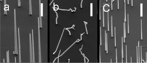
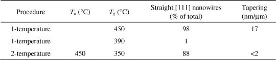
Fig. 1 illustrates FESEM images of some typical GaAs nanowires grown on GaAs substrates at various temperatures. Table 1 summarizes the growth temperature and key characteristics of GaAs nanowires grown in this study. Nanowires grown by the single- temperature procedure were generally straight and epitaxially aligned in the vertical [111]B direction when grown at Tg of 410 °C and above (Fig. 1a), but suffer severe tapering. At Tg of 390 °C and below (Fig. 1b), nanowire growth rarely initiated in the vertical [111]B direction, and subsequent kinking was common: the initial and final nanowire orientations exhibit no apparent relationship with the substrate. In contrast, the two-temperature procedure allowed the growth of straight, vertical [111]B-oriented nanowires at Tg as low as 350 °C (Fig. 1c). We determine a minimum Tn of 410 °C, and a minimum Tg of 350 °C are required for this straight epitaxial nanowire growth.10
Fig. 1. FESEM images of GaAs nanowires grown by single temperature and two-temperature procedures at various Tg. (a) Single-temperature procedure with Tg of 450 °C. (b) Single temperature procedure with Tg of 390 °C. (c) Two-temperature procedure with Tg of 350 °C (Tn of 450 °C). Samples are tilted at 40°. Scale bar is 2 μm.
Table 1. Summary of nanowire morphology for single- and two-temperature procedures with various growth temperatures (Tg). Tapering is calculated for straight nanowires only.
The temperature-dependent reduction in tapering is explained with reference to the axial and radial growt...