A CPU can do many different things, but it does nothing unless it is told to. It needs to be issued with instructions. The instructions are issued to it in the form of a program, stored in memory. The instructions that a given CPU can understand and obey are its instruction set.
Different types of CPU have a different instruction set; that is, they have a particular collection of instructions suited to the architecture of the CPU. Some kinds of CPU have a large instruction set with several hundred instructions in it (CISC). Others work on a much smaller set, usually fewer than a hundred (RISC). Usually all the members of a family of CPUs have the same instruction set. Some members of the family, especially the newer ones, may have a few additional instructions in their set.
The CPU obtains its instructions by going to an address in memory and reading the instructions stored there. There are very fast CPUs that read more than one at a time but most CPUs read one instruction at a time and act on it before fetching the next one. This is the type of CPU we describe in this chapter. We shall also confine our descriptions to systems in which the data is operated on as single bytes.
Fetch-execute cycle
When it is operating, a CPU repeatedly goes through a cycle known as the fetch-execute cycle. As its name implies, this cycle has two stages:
- The CPU fetches an instruction from memory.
- The CPU executes it, that is, it obeys the instruction.
The cycles are repeated continuously as the CPU works its way from the beginning of the program to the end.
The instruction is a byte of data stored in memory. Reading a byte from memory takes place in ten stages:
- The address of the byte to be read is transferred along the internal bus of the CPU to the address bus register.
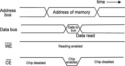
- The address is placed on the address bus (Fig. 7.1).
- The address is decoded by the logic (partly on the memory chip), to select the location for reading.
- Reading is enabled. In Fig. 7.1 the WRITE ENABLE line is already high so reading is already enabled.
- The CHIP ENABLE line goes low, to switch the memory chip outputs from the high-impedance state to a low-impedance state (outputs high or low).
- Data from the memory location appears on the data bus.
- The CPU stores the data from the bus in its data bus register.
- The data is transferred to the internal bus of the CPU.
- If the data is an instruction, it is stored in the instruction register.
- While the last two states are occurring, the CE line goes high and the data is no longer present on the data bus.
Assuming that the CPU has only one read-write enable control line.
Assuming that the data is an instruction, the logic of the control unit causes one of many different actions to occur.
Example:
The data register of an 8085 CPU holds the following byte:
01001111
Figure 7.1 Reading a byte from memory involves a sequence of logic levels on two lines of the control bus. The WRITE ENABLE line stays high as this is a read operation. Data from memory is put on the bus when the CHIP ENABLE line goes low.
| Test Your Knowledge 7.1 |
| What is the address put on the bus before the chip is enabled? |
The latches of the register are either set (= 1) or reset (= 0). When the control unit receives this data it copies to register C (a general-purpose register) the data that is in register A (the accumulator). This is an internal movement of data so a single byte is enough to tell the control unit what to do. How the control logic works, that is to say, how the input of 01001111 makes the control logic take the action we have described, is outside the scope of this book.
Remember that data transfer is by copying. The data now in the instruction register is still stored in memory, where it can be read as many times as the program requires.
Example:
At another time, the data register holds:
00110111
This instructs the control unit to set the carry bit of the status register to ‘1’. As above, a single byte is all that is necessary for this instruction. It is obvious that, if we always had to write out data as 8-bit binary numbers, as above, it would be all too easy to make mistakes. Instead, we express the numbers in hexadecimal. So the two instructions described above become:
4F, for copying data from A to C, and
37, for setting the carry bit
Some operations require two bytes. The first byte states what is to be done. On loading this byte, the CPU loads the next byte in memory to find out what value to operate on.
| Test Your Knowledge 7.2 |
| What is the code to make the CPU AND the contents of its register A with the value $2B? |
Example: The code E6 (actually 11100110) tells the control unit to AND register A with the binary value that is in the next byte. The control unit has to send the CPU back to memory to find out the value of this byte, which is stored in the next location to the instruction E6. Therefore, the full instruction might be:
E6 4A
This tells the control unit to AND the content of register A with the value 4A.
Writing to memory
A sequence of operations may often end in the storing of a result in memory. There are opcodes for storing the contents of various registers. The operand is the address at which the data is to be stored. In a 16-bit system, it takes two bytes to specify the address. This means that the opcode is followed by two bytes, making the instruction three bytes long. The sequence of storing data is almost the reverse of the sequence for reading data. It has nine stages:
- The address to which the byte is to be written is transferred along the internal bus of the CPU to the address bus register.
- The address is placed on the address bus (Fig. 7.2).
- The address is decoded by the logic (partly on the memory chip), to select the location for writi...