![]()
1
Introduction to Semiconductor Lithography
The fabrication of an integrated circuit (IC) involves a great variety of physical and chemical processes performed on a semiconductor (e.g. silicon) substrate. In general, the various processes used to make an IC fall into three categories: film deposition, patterning and semiconductor doping. Films of both conductors (such as polysilicon, aluminum, tungsten and copper) and insulators (various forms of silicon dioxide, silicon nitride and others) are used to connect and isolate transistors and their components. Selective doping of various regions of silicon allows the conductivity of the silicon to be changed with the application of voltage. By creating structures of these various components, millions (or even billions) of transistors can be built and wired together to form the complex circuitry of a modern microelectronic device. Fundamental to all of these processes is lithography, i.e. the formation of three-dimensional (3D) relief images on the substrate for subsequent transfer of the pattern into the substrate.
The word lithography comes from the Greek lithos, meaning stones, and graphia, meaning to write. It means quite literally writing on stones. In the case of semiconductor lithography, our stones are silicon wafers and our patterns are written with a lightsensitive polymer called a photoresist. To build the complex structures that make up a transistor and the many wires that connect the millions of transistors of a circuit, lithography and etch pattern transfer steps are repeated at least 10 times, but more typically 25 to 40 times to make one circuit. Each pattern being printed on the wafer is aligned to the previously formed patterns as slowly the conductors, insulators and selectively doped regions are built up to form the final device.
The importance of lithography can be appreciated in two ways. First, due to the large number of lithography steps needed in IC manufacturing, lithography typically accounts for about 30% of the cost of manufacturing a chip. As a result, IC fabrication factories (‘fabs’) are designed to keep lithography as the throughput bottleneck. Any drop in output of the lithography process is a drop in output for the entire factory. Second, lithography tends to be the technical limiter for further advances in transistor size reduction and thus chip performance and area. Obviously, one must carefully understand the trade-offs between cost and capability when developing a lithography process for manufacturing. Although lithography is certainly not the only technically important and challenging process in the IC manufacturing flow, historically, advances in lithography have gated advances in IC cost and performance.
1.1 Basics of IC Fabrication
A semiconductor is not, as its name might imply, a material with properties between an electrical conductor and an insulator. Instead, it is a material whose conductivity can be readily changed by several orders of magnitude. Heat, light, impurity doping and the application of an electric field can all cause fairly dramatic changes in the electrical conductivity of a semiconductor. The last two can be applied locally and form the basis of a transistor: by applying an electric field to a doped region of a semiconductor material, that region can be changed from a good to a poor conductor of electricity, or vice versa. In effect, the transistor works as an electrically controlled switch, and these switches can be connected together to form digital logic circuits. In addition, semiconductors can be made to amplify an electrical signal, thus forming the basis of analog solid-state circuits.
By far the most common semiconductor in use is silicon, due to a number of factors such as cost, formation of a stable native oxide and vast experience (the first silicon IC was built in about 1960). A wafer of single-crystal silicon anywhere from 75–300 mm in diameter and about 0.6–0.8 mm thick serves as the substrate for the fabrication and interconnection of planar transistors into an IC. The most advanced circuits are built on 200-and 300-mm-diameter wafers. The wafers are far larger than the ICs being made so that each wafer holds a few hundred (and up to a few thousand) IC devices. Wafers are processed in lots of about 25 wafers at a time, and large fabs can have throughputs of greater than 10000 wafers per week. The cycle time for making a chip, from starting bare silicon wafers to a finished wafer ready for dicing and packaging, is typically 30–60 days. Semiconductor processing (or IC fabrication) involves two major tasks:
- Creating small, interconnected 3D structures of insulators and conductors in order to manipulate local electric fields and currents
- Selectively doping regions of the semiconductor (to create p–n junctions and other electrical components) in order to manipulate the local concentration of charge carriers
1.1.1 Patterning
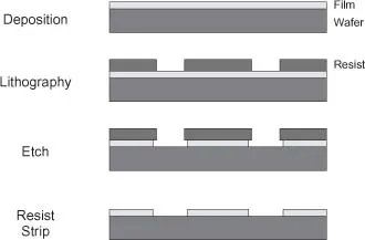
The 3D microstructures are created with a process called patterning. The common sub-tractive patterning process (Figure 1.1) involves three steps: (1) deposition of a uniform film of material on the wafer; (2) lithography to create a positive image of the pattern that is desired in the film; and (3) etch to transfer that pattern into the wafer. An additive process (such as electroplating) changes the order of these steps: (1) lithography to create negative image of the pattern that is desired; and (2) selective deposition of material into the areas not protected by the lithographically produced pattern. Copper is often patterned additively using the damascene process (named for a unique decorative metal fill process applied to swords and developed in Damascus about 1000 years ago).
Deposition can use many different technologies dependent on the material and the desired properties of the film: oxide growth (direct oxidation of the silicon), chemical vapor deposition (CVD), physical vapor deposition (PVD), evaporation and sputtering. Common films include insulators (silicon dioxide, silicon nitride, phosphorous-doped glass, etc.) and conductors (aluminum, copper, tungsten, titanium, polycrystalline silicon, etc.). Lithography, of course, is the subject of this book and will be discussed at great length in the pages that follow. Photoresists are classed as positive, where exposure to light causes the resist to be removed, and negative, where exposed patterns remain after development. The goal of the photoresist is to resist etching after it has been patterned so that the pattern can be transferred into the film.
1.1.2 Etching
Etch involves both chemical and mechanical mechanisms for removal of the material not protected by the photoresist. Wet etch, perhaps the simplest form of etch, uses an etchant solution such as an acid that chemically attacks the underlying film while leaving the photoresist intact. This form of etching is isotropic and thus can lead to undercutting as the film is etched from underneath the photoresist. If anisotropic etching is desired (and most always it is), directionality must be induced into the etch process. Plasma etching replaces the liquid etchant with a plasma - an ionized gas. Applying an electric field causes the ions to be accelerated downward toward the wafer. The resulting etch is a mix of chemical etching due to reaction of the film with the plasma and physical sputtering due to the directional bombardment of the ions hitting the wafer. The chemical nature of the etch can lead to good etch selectivity of the film with respect to the resist (selectivity being defined as the ratio of the film etch rate to the resist etch rate) and with respect to the substrate below the film, but is essentially isotropic. Physical sputtering is very directional (etching is essentially vertical only), but not very selective (the resist etches at about the same rate as the film to be etched). Reactive ion etching combines both effects to give good enough selectivity and directionality – the accelerated ions provide energy to drive a chemical etching reaction.
The photoresist property of greatest interest for etching is the etch selectivity, which is dependent both on the photoresist material properties and the nature of the etch process for the specific film. Good etch processes often have etch selectivities in excess of 4 (for example, polysilicon with a novolac resist), whereas poor selectivities can be as low as 1 (for example, when etching an organic bottom antireflection coating). Etch selectivity and the thickness of the film to be etched determine the minimum required resist thickness. Mechanical properties of the resist, such as adhesion to the substrate and resistance to mechanical deformation such as bending of the pattern, also play a role during etching.
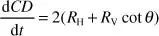
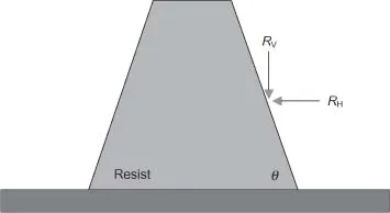
For an etch process without perfect selectivity, the shape and size of the final etched pattern will depend on not only the size of the resist pattern but its shape as well. Consider a resist feature whose straight sidewalls make an angle θ with respect to the substrate (Figure 1.2). Given vertical and horizontal etch rates of the resist RV and RH, respectively, the rate at which the critical dimension (CD) shrinks will be
Thus, the rate at which the resist CD changes during the etch is a function of the resist sidewall angle. As the angle approaches 90°, the vertical component ceases to contribute and the rate of CD change is at its minimum. In fact, Equation (1.1) shows three ways to minimize the change in resist CD during the etch: improved etch selectivity (making both RH and RV smaller), improved anisotropy (making RH/RV smaller) and a sidewall close to vertical (making cotθ smaller).
The example above, while simple, shows clearly how resist profile shape can affect pattern transfer. In general, the ideal photoresist shape has perfectly vertical sidewalls. Other nonideal profile shapes, such as rounding of the top of the resist and resist footing, will also affect pattern transfer.
1.1.3 Ion Implantation
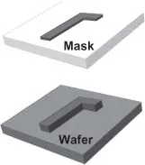
Selective doping of certain regions of the semiconductor begins with a patterning step (Figure 1.3). Regions of the semiconductor that are not covered by photoresist are exposed to a dopant impurity. p-type dopants like boron have three outer shell electrons and when inserted into the crystal lattice in place of silicon (which has four outer electrons) create mobile holes (empty spots in the lattice where an electron could go). n-type dopants such as phosphorous, arsenic and antimony have five outer electrons, which create excess mobile electrons when used to dope silicon. The interface between p-...