![]()
1
Introduction
1.1 Historical Perspective and Moore’s Law
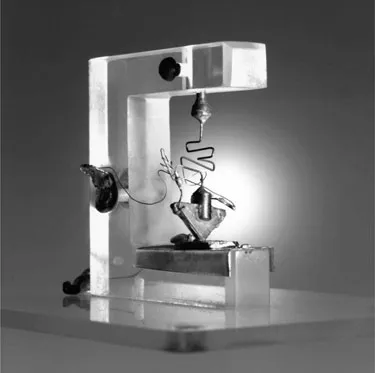
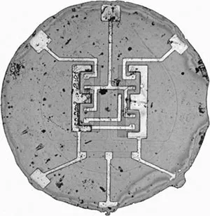
Since the demonstration of the first transistor [1,,2,3,4] at Bell Laboratories in 1947 (Figure 1.1), rapid progress in the design and manufacture of semiconductors has led to gigahertz microprocessors and gigabit memories today. The invention of the integrated circuit (Figure 1.2) in 1958 [5, 6], and subsequent improvements on the concept in the 1960s, made it possible to combine multiple devices on a single chip of silicon instead of wiring together devices on a circuit board. Thus, it was possible to reduce the size, weight, and cost of a circuit even while increasing its functionality. These breakthroughs eventually allowed the fabrication of billions of transistors in a single chip of silicon, enabling computing power far beyond that achievable by wiring together discrete transistors. At the present time, state-of-the-art microprocessor chips contain hundreds of millions of transistors, whereas memory chips contain up to several billion transistors.
FIGURE 1.1
The first transistor, invented at Bell Laboratories in 1947. (From Lucent Technologies Inc./Bell Labs. With permission.)
FIGURE 1.2
The first commercial integrated circuit, developed by Robert Noyce at Fairchild Semiconductor. The integrated circuit was invented by Robert Noyce of Fairchild Semiconductor and Jack Kilby of Texas Instruments at about the same time. (From Fairchild Semiconductor. With permission.)
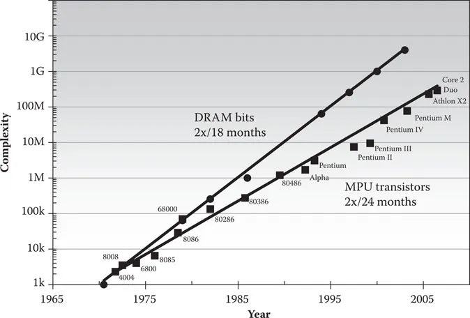
Soon after the realization of integrated circuits, Intel cofounder Gordon Moore noted that the complexity of integrated circuits was increasing exponentially with time. Moore stated that the “complexity” of integrated circuits with “minimum component costs” was doubling every 12 months [7]. Since that time, several variations of “Moore’s law” have been stated. Usually, it is noted that the number of transistors per microprocessor chip doubles every 24 months, whereas the number of bits per dynamic random access memory (DRAM) chip doubles every 18 months. Remarkably, this rate of progress has been maintained for more than three decades Figure 1.3 illustrates this exponential progress for microprocessors and DRAMs. Similar exponential trends have been established for flash memories and application-specific integrated circuits (ASICs). However, memory chips have outpaced microprocessors because of their simpler designs and built-in redundancy.
Industry has kept pace with Moore’s law primarily by scaling down the dimensions of transistors through improved lithography [8, 9], but chip size has also been increased. Transistor miniaturization has been pursued aggressively and has brought about improvements in circuit performance and cost as well as density. A key parameter describing this scaling is the “minimum feature size” for the transfer of circuit patterns from a computer design to the semiconductor wafer. Figure 1.4 shows the historical evolution of the minimum feature size, along with projections out to the year 2020. Historically, much of the progress shown in Figure 1.4 was achieved by decreasing the wavelength used in lithographic tools. However, at the present time, technical solutions for the lithographic requirements of 2020 and beyond have not been found.
FIGURE 1.3
According to Moore’s law, the complexity of integrated circuits has increased exponentially with time. Historically, the number of transistors per microprocessor unit (MPU) doubles every 24 months; the number of bits per DRAM chip doubles every 18 months.
With the goal of extending the historic trends in integrated circuit technology, the Semiconductor Industry Association in the United States [10] produced the National Technology Roadmap for Semiconductors in 1992. This roadmap defined industry-wide technology goals with a 15-year horizon and was revised in 1994 and 1997. In 1998, after the globalization of the semiconductor industry, an International Technology Roadmap for Semiconductors (ITRS) was developed with participation from the semiconductor industries in Europe, Japan, Korea, and Taiwan [11]. Full ITRS reports are published biannually, in odd years, and update reports are published in even years.
Each ITRS report projects industry trends 15 years into the future. What, then, is the digital integrated circuit industry expected to look like in 2020? According to the 2007 ITRS, the starting silicon wafers will grow to 450 mm in diameter, whereas transistor gate lengths will diminish to 5.6 nm. As a consequence of these developments, flash memory will be able to store one terabit on a single chip, and you will be able to purchase a 12.4 GHz processor with 6.1 billion transistors and 7902 pins for about 0.24 microcents per transistor These and other important trends are charted in Table 1.1.