![]()
Part One
Fundamentals
![]()
1
Overview of Micro Cutting
Dehong Huo1 and Kai Cheng2
1 School of Mechanical and Systems Engineering, Newcastle University
2 School of Engineering and Design, Brunel University
1.1 Background and Scope
1.1.1 Micro Manufacturing
The increasing demands on micro and miniature parts, components and systems have led to the development of micro and nanotechnology. It is well-recognized that micro manufacturing has been a key enabling technology in industrially producing useful micro products and processes.
Micro Electric Mechanical Systems (MEMS) or micro system technology (MST) as known in Europe has been booming over the last two decades or so. Numerous MEMS products mainly micro sensors and micro actuators using silicon have been fabricated. These MEMS sensors and actuators have been widely used in various applications including medical engineering (e.g. pressure sensors), communications (high frequency resonators), inertial sensing (e.g. accelerometers and gyroscopes), to name a few. The processes employed to fabricate MEMS devices and other microelectronics products can be described as MEMS micro manufacturing or lithography-based micro manufacturing. Common techniques include photolithography, chemical-etching, plating and LIGA, and so on. Lithography-based micro manufacturing has existed and been developed for many years and is regarded as a mature large volume production process, hence the term micro manufacturing is familiar in the semiconductor or microelectronics fields.
In the past 20 years or so, high-accuracy complex shape micro and miniature components made from a range of engineering materials are increasingly in demand for various engineering industries. The geometry and functional requirements have led to the development of another category of micro manufacturing techniques termed as non-MEMS micro manufacturing or non-lithography-based micro manufacturing, which are fundamentally different from MEMS micro manufacturing in many aspects.
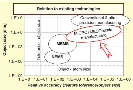
Non-lithography-based micro manufacturing is a relatively new area, its concept, theories, processes and applications have been developed and formulated in the past around two decades. A report published by the WTEC panel on micro manufacturing describes non-lithography-based micro manufacturing as the creation of high-precision three dimensional products using a variety of materials and possessing features with sizes ranging from tens of micrometers to a few millimeters (WETC report). Figure 1.1 illustrates micro manufacturing size/precision domains. Micro manufacturing is normally used to produce part or feature size ranging from tens or hundreds of microns. Although micro manufacturing may not be capable of producing the smallest feature size as would be the case using MEMS and NEMS (Nano Electric Mechanical Systems) processes, it is a critical technology in bridging the gap between macro and nano domain [1]. It has many advantages over lithography-based micro manufacturing processes in terms of material choices, relative accuracy and the complexity of part geometry.
Typically non-lithography-based micro manufacturing includes micro EDM, micro mechanical-cutting, laser-cutting/patterning/drilling, micro-extrusion, micro-embossing, micro stamping, micro-injection moulding, and so on. These processes are based on different working principles and have their own respective characteristics in terms of production rate, attainable accuracy and surface finishes, and so on. But they are capable of producing 3D shape geometry micro parts over a wider range of engineering materials. This book will only focus on the micro mechanical-cutting process. Table 1.1 highlights the difference between MEMS micro manufacturing and non-MEMS micro manufacturing techniques (using mechanical micro machining as an example) to compare the fundamental differences between the two category micro manufacturing processes.
From Table 1.1 it can be found that micro mechanical machining has many advantages over MEMS-based process, such as wider materials choices, higher accuracy and capability of producing complex 3D geometry micro parts.
Recently, significant research efforts have been made on non-lithography-based micro manufacturing techniques. Europe has invested heavily in the research and development in micro manufacturing. In the past decade, dozens of EU large Framework projects have been initiated, such as MASMICRO, 4M, Launch-Micro, Production4ì, EUPASS, Hydromel, HYTI, NANOSAFE2, Manudirect, Napolyde, PRONANO, NaPa, CHARPAN, NANOIMPRINT, and so on. These projects cover all areas in micro and nano manufacturing, precision manufacturing and metrology [2]. In a study conducted by the UK Technology Strategy Board (TSB) on high value manufacturing in the UK, micro and nano manufacturing processes are identified as one of the most significant emerging manufacturing processes which would address challenges for the UK high value manufacturing industry [3].
Table 1.1 Comparisons between MEMS -based process and micro machining
|
| Workpiece materials | Silicon, some metals | Metals, alloys, polymers, composite, technical ceramics |
| Component geometry | Planer or 2.5D | Complex 3D |
| Assembly methods | None or bonding | Fastening, welding, bonding |
| Relative accuracy | 10-1–10-3 | 10-3–10-5 |
| Process control | Feedforward | Feedback |
| Machine size | Macro | Macro to micro |
| Production volume | High | High or low |
| Production rate | High | Low |
| Initial investment | High | Intermediate or low |
| Applications | MEMS, microelectronics, some planner micro parts | Various applications requiring 3D micro components |
1.1.2 History and Development Process of Micro Cutting
Micro cutting as an emerging subject area in its own right has attracted growing attention from both researchers and industry in the last two decades. Because mechanical cutting is a well-established area much knowledge from macro cutting has thus been adapted to study micro cutting processes. Some researchers from the conventional mechanical cutting research community shifted their research interests to micro-domain. Basically there are two research approaches being taken to study micro cutting. One approach is miniaturization of the conventional cutting process, tooling and equipment with an emphasis on their scaling down effect. The other approach can find its origin in ultra-precision machining, especially single point diamond turning (SPDT) with the emphasis on cutting mechanics, although the two approaches overlap in some areas and attempt to address similar issues, such as cutting tool edge size effect, minimum chip thickness, and so on.
The approach of miniaturization of the conventional cutting process tends to be process parameters centric. Macro-phenomena such as machining dynamics, chatters, cutting forces, and so on are directly translated into the micro-domain and the machine-tool interaction effect is well considered and modelled. Macro analytical, mechanistic and numerical cutting process models are adapted to micro cutting with consideration of the so called size effect.
The other approach utilizes research output from ultra-precision diamond cutting and tends to be cutting mechanics centric in nature. This approach is similar to diamond cutting research, but studies micro cutting, with more emphasis on tool geometries, material crystalline orientation and micro structures. Machine dynamics are often neglected as cutting forces are given very little consideration so that ultra-precision machines are treated as rigid and their effects do not appeared in the models. Atomic scale simulation or other numerical modelling considering micro structure and grain size effects are used for this approach and study.
As discussed above, traditionally MEMS and microelectronics use silicon materials-based micro manufacturing processes which are fundamentally different from mechanical micro cutting. With the increasing requirement on 3D complex shape MEMS devices, mechanical micro cutting will have great potential to fabricate micro parts for MEMS and microelectronics applications. On the other hand, hybrid micro manufacturing approaches, for example, a combination of micro cutting and etching processes to fabricate high precision 3D micro parts, is likely to be a promising method.
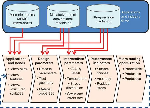
Figure 1.2 highlights a typical micro cutting development process, starting from applications and needs which come from microelectronics and MEMS, miniaturization of conventional machining and ultra-precision machining; a micro cutting development flow has a number of key stages. Design parameters including process parameters (e.g. cutting speed, uncut chip thickness, feedrate), tool geometry, material properties, and so on will be developed ...