- English
- ePUB (mobile friendly)
- Available on iOS & Android
eBook - ePub
About this book
Since its discovery in 2004, graphene has been a great sensation due to its unique structure and unusual properties, and it has only taken
6 years for a Noble Prize to be awarded for the field of graphene research. This monograph gives a well-balanced overview on all areas of
scientific interest surrounding this fascinating nanocarbon. In one handy volume it offers comprehensive coverage of the topic, including
chemical, materials science, nanoscience, physics, engineering, life science, and potential applications. Other graphene-like, inorganic layered materials are also discussed.
Edited by two highly honored scientists, this is an invaluable companion for inorganic, organic, and physical chemists, materials scientists,
and physicists.
From the Contents:
* Synthesis, Characterization, and Selected Properties of Graphene
* Understanding Graphene via Raman Scattering
* Physics of Quanta and Quantum Fields in Graphene
* Graphene and Graphene-Oxide-Based Materials for Electrochemical Energy Systems
* Heterogeneous Catalysis by Metal Nanoparticles supported on Graphene
* Graphenes in Supramolecular Gels and in Biological Systems
and many more
Tools to learn more effectively

Saving Books

Keyword Search

Annotating Text

Listen to it instead
Information
Chapter 1
Synthesis, Characterization, and Selected Properties of Graphene
1.1 Introduction
Carbon nanotubes (CNTs) and graphene are two of the most studied materials today. Two-dimensional graphene has specially attracted a lot of attention because of its unique electrical properties such as very high carrier mobility [1–4], the quantum Hall effect at room temperature [2, 5], and ambipolar electric field effect along with ballistic conduction of charge carriers [1]. Some other properties of graphene that are equally interesting include its unexpectedly high absorption of white light [6], high elasticity [7], unusual magnetic properties [8, 9], high surface area [10], gas adsorption [11], and charge-transfer interactions with molecules [12, 13]. We discuss some of these aspects in this chapter. While graphene normally refers to a single layer of sp2 bonded carbon atoms, there are important investigations on bi- and few-layered graphenes (FGs) as well. In the very first experimental study on graphene by Novoselov et al. [1, 2] in 2004, graphene was prepared by micromechanical cleavage from graphite flakes. Since then, there has been much progress in the synthesis of graphene and a number of methods have been devised to prepare high-quality single-layer graphenes (SLGs) and FGs, some of which are described in this chapter.
Characterization of graphene forms an important part of graphene research and involves measurements based on various microscopic and spectroscopic techniques. Characterization involves determination of the number of layers and the purity of sample in terms of absence or presence of defects. Optical contrast of graphene layers on different substrates is the most simple and effective method for the identification of the number of layers. This method is based on the contrast arising from the interference of the reflected light beams at the air-to-graphene, graphene-to-dielectric, and (in the case of thin dielectric films) dielectric-to-substrate interfaces [14]. SLG, bilayer-, and multiple-layer graphenes (<10 layers) on Si substrate with a 285 nm SiO2 are differentiated using contrast spectra, generated from the reflection light of a white-light source (Figure 1.1a) [15]. A total color difference (TCD) method, based on a combination of the reflection spectrum calculation and the International Commission on Illumination (CIE) color space is also used to quantitatively investigate the effect of light source and substrate on the optical imaging of graphene for determining the thickness of the flakes. It is found that 72 nm thick Al2O3 film is much better at characterizing graphene than SiO2 and Si3N4 films [16].
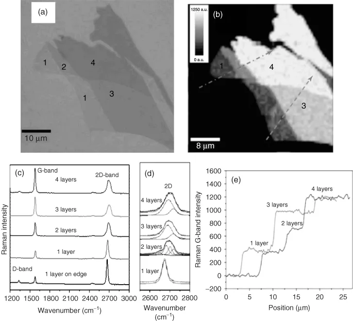
Figure 1.1 (a) Optical image of graphene with one, two, three, and four layers; (b) Raman image plotted by the intensity of G-band; (c) Raman spectra as a function of the number of layers; (d) zoom-in view of the Raman 2D-band; and (e) the cross section of the Raman image, which corresponds to the dashed lines in (b).
(Source: Reprinted with permission from Ref. [15].)
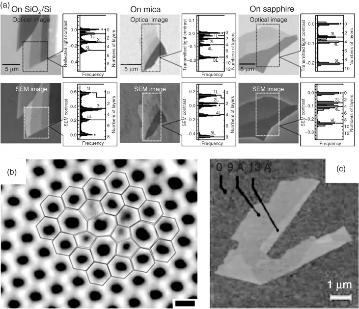
Contrast in scanning electron microscopic (SEM) images is another way to determine the number of layers. The secondary electron intensity from the sample operating at low electron acceleration voltage has a linear relationship with the number of graphene layers (Figure 1.2a) [17]. A quantitative estimation of the layer thicknesses is obtained using attenuated secondary electrons emitted from the substrate with an in-column low-energy electron detector [18]. Transmission electron microscopy (TEM) can be directly used to observe the number of layers on viewing the edges of the sample, each layers corresponding to a dark line. Gass et al. [19] observed individual atoms in graphene by high-angle annular dark-field (HAADF) scanning transmission electron microscopy (STEM) in the aberration-corrected mode at an operation voltage of 100 kV. Direct visualization of defects in the graphene lattice, such as the Stone–Wales defect, has been possible by aberration-corrected TEM with monochromator (Figure 1.2b) [20]. Electron diffraction can be used for differentiating the single layer from multiple layers of graphene. In SLG, there is only the zero-order Laue zone in the reciprocal space, and the intensities of diffraction peaks do not therefore, change much with the incidence angle. In contrast, bilayer graphene exhibits changes in total intensity with different incidence angles. Thus, the weak monotonic variation in diffraction intensities with tilt angle is a reliable way to identify monolayer graphene [21]. The relative intensities of the electron diffraction pattern from the {2110} and {1100} planes can be used to determine the number of layers. If I{1100}/I{2110} is >1, it is reported as SLG, and if the ratio is <1, it is multilayer graphene [22]. Thickness of graphene layers can be directly probed by atomic force microscopy (AFM) in tapping mode. On the basis of the interlayer distance in graphite of 3.5 Å [3], the thickness of a graphene flake or the number of layers is determined as shown in Figure 1.2c [3]. Scanning tunneling microscopy (STM) also provides high-resolution images of graphene.
Figure 1.2 (a) Comparison of the counting of layers by optical microscopy and SEM for graphene on SiO2/Si, mica, and sapphire. For each figure is shown a histogram of the distribution of graphene layers within the rectangular area indicated by a dotted line. (Source: Reprinted with permission from Ref. [17].) (b) High-resolution transmission electron microscopic image showing the Stone–Wales defects in graphene. (Source: Reprinted with permission from Ref. [20].) (c) Atomic force microscopic image of single-layered graphene. Folded edge shows a height increase of 4 Å indicating single-layer graphene.
(Source: Reprinted with permission from Ref. [3].)
Raman spectroscopy has been extensively used as a nondestructive tool to probe the structural and electronic characteristics of graphene [3]. Figure 1.1c shows typical Raman spectra of one-, two-, three-, and four-layered graphene prepared using micromechanical cleavage technique and placed on SiO2/Si substrate. The Raman spectrum of graphene has three major bands. The D-band located around 1300 cm−1 is a defect-induced band. The G-band located around 1580 cm−1 is due to in-plane vibrations of the sp2 carbon atoms. The 2D-band around 2700 cm−1 results from a second-order process. The appearance of the D- and 2D-bands is related to the double resonance Raman scattering process [23], and with the increasing the number of layers, the 2D-band gets broadened and blue shifted. A sharp and symmetric 2D-band is found in the case of SLG as shown in Figure 1.1d. The Raman image obtained from the intensity of the G-band is shown in Figure 1.1b. A linear increase in the intensity profile of the G-band with increase in the number of layers along the dashed line is shown in Figure 1.1e [15]. Surface area, which also forms an important characteristic of graphene, is discussed later in the chapter.
1.2 Synthesis of Single-Layer and Few-Layered Graphenes
SLG and FG have been synthesized by several methods. In Table 1.1, we have listed some of these methods. The synthesis procedure can be broadly classified into exfoliation, chemical vapor deposition (CVD), arc discharge, and reduction of graphene oxide.
Table 1.1 Synthesis of Single- and Few-Layered Graphene
| Graphene synthesis | |
| Single layer | Few layers |
| Micromechanical cleavage of HOPG | Chemical reduction of exfoliated graphene oxide (2–6 layers) |
| CVD on metal surfaces | |
| Epitaxial growth on an insulator (SiC) | Thermal exfoliation of graphite oxide (2–7 layers) |
| Intercalation of graphite | Aerosol pyrolysis (2–40 layers) |
| Dispersion of graphite in water, NMP | |
| Reduction of single-layer graphene oxide | Arc discharge in presence of H2 (2–4 layers) |
1.2.1 Mechanical Exfoliation
Stacking of sheets in graphite is the result of overlap of partially filled pz or π orbital perpendicular to the plane of the sheet (involving van der Waals forces). Exfoliation is the reverse of stacking; owing to the weak bonding and large lattice spacing in the perpendicular direction compared to the small lattice spacing and stronger bonding in the hexagonal lattice plane, it has been tempting to generate graphene sheets through exfoliation of graphite (EG). Graphene sheets of different thickness can indeed be obtained through mechanical exfoliation or by peeling off layers from graphitic materials such as highly ordered pyrolytic graphite (HOPG), single-crystal graphite, or natural graphite. Peeling and manipulation of graphene sheets have been achieved through AFM and STM tips [24–29]. Greater control over folding and unfolding could be achieved by modulating the distance or bias voltage between the tip and the sample [29]. Zhang [30] obtained 10–100 nm thick graphene sheets using graphite island attached to tip of micromachined Si cantilever to scan over SiO2/Si surface. Folding and tearing of the sheets arise due to the formation of sp3-like line defects in the sp2 graphitic network, occu...
Table of contents
- Cover
- Related Titles
- Title Page
- Copyright
- Preface
- List of Contributors
- Chapter 1: Synthesis, Characterization, and Selected Properties of Graphene
- Chapter 2: Understanding Graphene via Raman Scattering
- Chapter 3: Physics of Quanta and Quantum Fields in Graphene
- Chapter 4: Magnetism of Nanographene
- Chapter 5: Physics of Electrical Noise in Graphene
- Chapter 6: Suspended Graphene Devices for Nanoelectromechanics and for the Study of Quantum Hall Effect
- Chapter 7: Electronic and Magnetic Properties of Patterned Nanoribbons: A Detailed Computational Study
- Chapter 8: Stone–Wales Defects in Graphene and Related Two-Dimensional Nanomaterials
- Chapter 9: Graphene and Graphene-Oxide-Based Materials for Electrochemical Energy Systems
- Chapter 10: Heterogeneous Catalysis by Metal Nanoparticles Supported on Graphene
- Chapter 11: Graphenes in Supramolecular Gels and in Biological Systems
- Chapter 12: Biomedical Applications of Graphene: Opportunities and Challenges
- Index
Frequently asked questions
Yes, you can cancel anytime from the Subscription tab in your account settings on the Perlego website. Your subscription will stay active until the end of your current billing period. Learn how to cancel your subscription
No, books cannot be downloaded as external files, such as PDFs, for use outside of Perlego. However, you can download books within the Perlego app for offline reading on mobile or tablet. Learn how to download books offline
Perlego offers two plans: Essential and Complete
- Essential is ideal for learners and professionals who enjoy exploring a wide range of subjects. Access the Essential Library with 800,000+ trusted titles and best-sellers across business, personal growth, and the humanities. Includes unlimited reading time and Standard Read Aloud voice.
- Complete: Perfect for advanced learners and researchers needing full, unrestricted access. Unlock 1.4M+ books across hundreds of subjects, including academic and specialized titles. The Complete Plan also includes advanced features like Premium Read Aloud and Research Assistant.
We are an online textbook subscription service, where you can get access to an entire online library for less than the price of a single book per month. With over 1 million books across 990+ topics, we’ve got you covered! Learn about our mission
Look out for the read-aloud symbol on your next book to see if you can listen to it. The read-aloud tool reads text aloud for you, highlighting the text as it is being read. You can pause it, speed it up and slow it down. Learn more about Read Aloud
Yes! You can use the Perlego app on both iOS and Android devices to read anytime, anywhere — even offline. Perfect for commutes or when you’re on the go.
Please note we cannot support devices running on iOS 13 and Android 7 or earlier. Learn more about using the app
Please note we cannot support devices running on iOS 13 and Android 7 or earlier. Learn more about using the app
Yes, you can access Graphene by C. N. R. Rao,Ajay K. Sood in PDF and/or ePUB format, as well as other popular books in Physical Sciences & Inorganic Chemistry. We have over one million books available in our catalogue for you to explore.