![]()
Chapter 1
Introduction
1.1 Surface and Interfaces in Everyday Life
Surfaces and interfaces are all around us. Their properties are important in our daily lives and are basic to many of today’s advanced technologies. This is particularly true for the semiconductor materials that are used throughout modern electronics. The aim of this book is to present the physical principles underlying the electronic, chemical, and structural properties of semiconductor interfaces and the techniques available to characterize them. Surfaces and interfaces are a cross-disciplinary field of science and engineering. As such, this book emphasizes the principles common to physics, electrical engineering, materials science, and chemistry as well as the links between fundamental and practical issues.
Surfaces and interfaces play a central role in numerous everyday phenomena. These include (i) triboelectricity, the transfer of charge between two materials brought into contact – such as the static electricity built up on a comb after combing one’s hair; (ii) corrosion, the oxidation of structural materials used in, for example, buildings, bridges, and aircraft; (iii) passivation, the prevention of such chemical or biological processes using special protective layers; (iv) colloid chemistry, the wetting of surfaces and the dispersion of particles within fluids as emulsions or colloids, for example, paints and time-release capsule medicines; (v) tribology, the friction between sliding objects in contact and their interface lubrication; (vi) cleaning and chemical etching, the removal of surface layers or adsorbed species; (vii) catalysis, the reduction in energetic barriers to speed up or improve the yield of chemical reactions, for example, refining oil or burning coal; and (viii) optical interference, the rainbow of colors reflected off thin oil layers or the internal reflection of light between stacks of materials only a few wavelengths of light thick. On a much larger scale are (ix) electromagnetic interfaces between the earth’s atmospheric layers that bounce short-wave radio signals around the world and that alter the reflection or absorption of sunlight contributing to global warming.
1.2 Surfaces and Interfaces in Electronics Technology
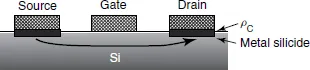
Surfaces and interfaces are fundamental to microelectronics. One of the most important microelectronic devices is the transistor, all functions of which depend on the boundaries between electronic materials. Figure 1.1 illustrates the three aspects of this dependence. Here, current passes from a source metal to a drain metal through a semiconductor, in this case, silicon (Si). A gate metal between the source and the drain is used to apply voltages that attract or repel the charge carriers involved in the current flow. The result is control or “gating” of the current flow by this third electrode. This basic device element is at the heart of the microelectronics industry.
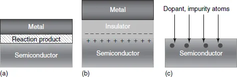
The surfaces and interfaces are the key to the transistor’s operation, shown in Figure 1.1. Thus, the contact between the metal and Si is a metal silicide. Barriers can form between metals and semiconductors that impede charge movement and introduce voltage drops across their interfaces. This barrier formation is a central topic of this book. Microelectronics researchers found that promoting a chemical reaction to form silicides, such as TiSi2 between Ti and Si, reduces such transport barriers and the contact resistivity ρc at these metal–semiconductor interfaces. This is illustrated, for example, in Figure 1.2a. Such interfacial silicide layers form low resistance, planar interfaces that can be integrated into the manufacturing process. A challenge of this approach is to achieve very thin, low ρc contacts without allowing reactions to extend far away from the junction.
The second important interface appears at the gate–semiconductor junction, shown in Figure 1.2b. Here, the earliest transistor experiments [1] showed the presence of fixed charges at this interface that prevented control of the source–drain current. This gate interface may involve a metal in direct contact with the semiconductor or, more commonly, a stack of metal-on-insulator-on semiconductor to apply voltage bias without introducing additional current. Atomic sites within the insulator and its semiconductor interface can immobilize charge and introduce dipoles across the insulator–semiconductor interface. This localized charge produces a voltage drop that offsets applied voltages at the gate metal, opposing the gate’s control of the source–drain current flow. Minimizing the formation of these localized charge sites has been one of the prime goals of the microelectronics industry since the invention of the transistor.
The third important microelectronic interface involves diffusion of atoms into and out of the semiconductor. Atomic diffusion of atoms into the semiconductor that donate or accept charge is used to control the concentration of free charge carriers within specific regions of a device. Acceleration and implantation of ionized atoms is a common process to achieve such doped layers that extend into semiconductor surfaces, here illustrated in Figure 1.2c. In addition, atomic diffusion can occur between two materials in contact that are annealed at high temperature. High-temperature annealing is often used to heal lattice damage after implantation or to promote reactions at particular device locations. However, such annealing can introduce diffusion and unintentional doping at other regions of the device. Outdiffusion of semiconductor constituents is also possible, resulting in native point defects that can also be electrically active. Balancing these effects requires careful design of materials, surface and interface preparation, thermal treatment, and device architectures.
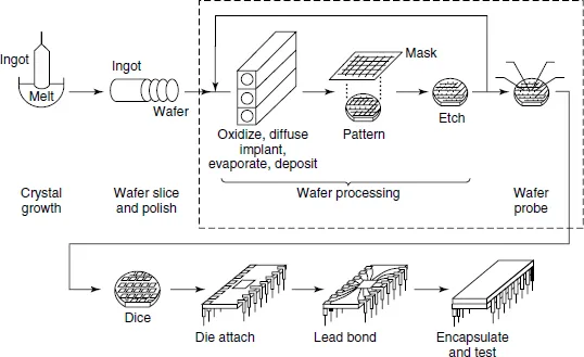
Microelectronic circuits consist of many interfaces between semiconductors, oxides, and metals. Figure 1.3 illustrates how these interfaces form as silicon progresses from its melt-grown crystal boule to a packaged chip. The Si boule formed by pulling the crystal out of a molten bath is sectioned into wafers, which are then oxidized, diffused, or implanted with dopants, and overcoated with various metal and organic layers. Photolithography is used to pattern and etch these wafers into monolithic arrays of devices. The wafer is then diced into individual circuits that are then mounted, wire bonded, and packaged into chips.
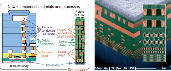
Within each circuit element, there can be many layers of interconnected conductors, insulators, and their interfaces. Figure 1.4 illustrates the different materials and interfaces associated with a 0.18−μm transistor at the bottom of a multilayer Al–W–Si-oxide dielectric assembly [2]. Reaction, interdiffusion, and formation of localized states must all be carefully controlled at all of these interfaces during the many patterning, etching, and annealing steps involved in assembling the full structure. Figure 1.4 also shows that materials and geometries change to compensate for the otherwise increasing electrical resistance as interconnects between layers shrink into the nanoscale regime. This continuing evolution in microelectronics underscores the importance of interfaces since the material volume associated with these interfaces becomes a larger proportion of the entire structure as circuit sizes decrease.
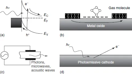
Many other conventional electronic devices rely on interfaces for their operation. Figure 1.5a illustrates the interface between a metal and semiconductor within a solar cell schematically as an energy E versus distance × band diagram. The Fermi levels EF in the metal (solid line) and the semiconductor (dashed line) align at a constant energy, whereas the conduction band EC and the valence band EV in the semiconductor bend near the interface. Incident photons of energy hν at this interface create electrons and holes that separate under the field set up by these bent bands. This charge separation results in photoinduced current or voltage between the metal and the semiconductor.
Figure 1.5b shows what appears to be a transistor structure except that, unlike Figure 1.1, there is no gate. Instead, molecules on this otherwise free surface adsorb on the surface, exchanging charge and inducing a field analogous to that of a gate. Figure 1.5c illustrates a circuit that generates photon, microwaves, or acoustic waves. The contacts that inject current or apply voltage to the generator layer are key to its practical operation. Unless the resistance of such contacts is low, power is lost at these contacts, reducing or totally blocking power conversion inside the semiconductor. Figure 1.5d illustrates an interface involving just a semiconductor surface that emits electrons when excited by incident photons. Chemical treatment of selected semiconductors enables these surfaces to emit multiple electrons when struck by single photons. Such surfaces are useful as electron pulse generators or photomultipliers.
Surfaces and interfaces have an even larger impact on electronics as devices move into the quantum regime. Figure 1.6 illustrates four such quantum electronic devices schematically. Figure 1.6a illustrates the energy band diagram of a quantum well, one of the basic components of optoelectronics. Here, the decrease in bandgap between EC and EV of one semiconductor sandwiched between layers of a larger bandgap semiconductor localizes both electrons and holes in the smaller gap material. This joint localization enhances electron–hole pair recombination and light emission. The quantum well is typically only a few atomic layers thick so that the allowed energies ...