Optical Processes in Semiconductors
eBook - ePub

Optical Processes in Semiconductors

  1. 448 pages
  2. English
  3. ePUB (mobile friendly)
  4. Available on iOS & Android
eBook - ePub

Optical Processes in Semiconductors

Book details
Book preview
Table of contents
Citations

About This Book

Based on a series of lectures at Berkeley, 1968–1969, this is the first book to deal comprehensively with all of the phenomena involving light in semiconductors. The author has combined, for the graduate student and researcher, a great variety of source material, journal research, and many years of experimental research, adding new insights published for the first time in this book.
Coverage includes energy states in semiconductors and their perturbation by external parameters, absorption, relationships between optical constants, spectroscopy, radiative transitions, nonradiative recombination, processes in pn junctions, semiconductor lasers, interactions involving coherent radiation, photoelectric emission, photovoltaic effects, polarization effects, photochemical effects, effect of traps on luminescence, and reflective modulation.
The author has presented the subject in a manner which couples readily to physical intuition. He introduces new techniques and concepts, including nonradiative recombination, effects of doping on optical properties, Franz-Keldysh effect in absorption and emission, reflectance modulation, and many others. Dr. Pankove emphasizes the underlying principle that can be applied to the analysis and design of a wide variety of functional devices and systems. Many valuable references, illustrative problems, and tables are also provided here.

Frequently asked questions

Simply head over to the account section in settings and click on ā€œCancel Subscriptionā€ - itā€™s as simple as that. After you cancel, your membership will stay active for the remainder of the time youā€™ve paid for. Learn more here.
At the moment all of our mobile-responsive ePub books are available to download via the app. Most of our PDFs are also available to download and we're working on making the final remaining ones downloadable now. Learn more here.
Both plans give you full access to the library and all of Perlegoā€™s features. The only differences are the price and subscription period: With the annual plan youā€™ll save around 30% compared to 12 months on the monthly plan.
We are an online textbook subscription service, where you can get access to an entire online library for less than the price of a single book per month. With over 1 million books across 1000+ topics, weā€™ve got you covered! Learn more here.
Look out for the read-aloud symbol on your next book to see if you can listen to it. The read-aloud tool reads text aloud for you, highlighting the text as it is being read. You can pause it, speed it up and slow it down. Learn more here.
Yes, you can access Optical Processes in Semiconductors by Jacques I. Pankove in PDF and/or ePUB format, as well as other popular books in Physical Sciences & Physics. We have over one million books available in our catalogue for you to explore.

Information

Year
2012
ISBN
9780486138701

ENERGY STATES IN SEMICONDUCTORS

1

In this chapter we shall sketch how the assemblage of similar atoms into an array leads to the formation of bands of allowed states separated by an energy gap. Then we shall show that the energy gap can be filled with a great variety of allowed states, some localized due to impurities and others permeating the crystal (excitons). We shall also describe how the various particles can interact to form complexes.
The relevance of these levels to the optical properties of the semiconductors lies in the fact that optical effects deal with transitions between various states and, therefore, it is well to review these first and to see how they come about.

1-A Band Structure

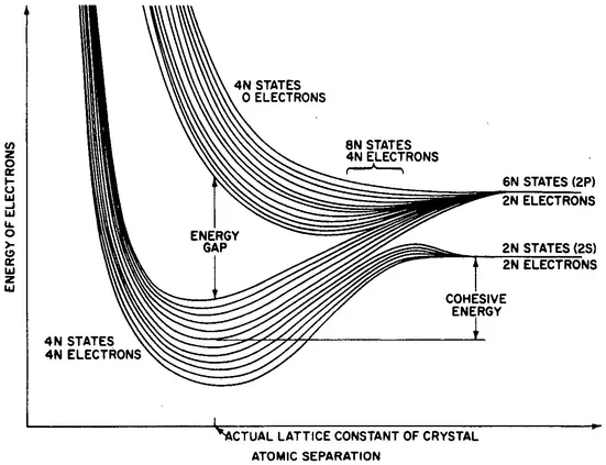
1-A-1 BANDING OF ATOMIC LEVELS

To understand the nature of semiconductors one must consider what happens when similar atoms are brought together to form a solid such as a crystal. As two similar atoms approach each other the wave functions of their electrons begin to overlap. To satisfy Pauliā€™s exclusion principle, the states of all spin-paired electrons acquire energies which are slightly different from their values in the isolated atom. Thus if N atoms are packed within a range of interaction, 2N electrons of the same orbital can occupy 2N different states, forming a band of states instead of a discrete level as in the isolated atom.
The energy distribution of the states depends strongly on the interatomic distance. This is illustrated in Fig. 1-1 for an assemblage of carbon atoms. The lowest-energy states are depressed to a minimum value when the diamond crystal is formed. The average amount by which the potential energy has dropped is related to the cohesive energy of the crystal. Notice that some of the higher-energy states (2P) merge with the band of 2S states. As a result of this mixing of states, the lower band contains as many states as electrons. This band is called the valence band and is characterized by the fact that it is completely filled with electrons. Such a filled band cannot carry a current. The upper band of states, which contains no electron, is called the conduction band. If an electron were placed in this band, it could acquire a net drift under the influence of an electric field.
e9780486138701_i0002.webp
Fig. 1-1 Energy banding of allowed levels in diamond as a function of spacing between atoms.1
Clearly, since in the energy gap there are no allowed states, one would not expect to find an electron within that range of energies.
It is the extent of the energy gap and the relative availability of electrons that determine whether a solid is a metal, a semiconductor, or an insulator. In a semiconductor the energy gap usually extends over less than about three electron-volts and the density of electrons in the upper band (or of holes in the lower band) is usually less than 1020 cm-3. By contrast, in a metal the upper band is populated with electrons far above the energy gap and the electron concentration is of the order of 1023 cm-3. Insulators, on the other hand, have a large energy gapā€”usually greater than 3 eVā€”and have a negligible electron concentration in the upper band (and practically no holes in the lower band).
Since the interatomic distance in a crystal is not isotropic but rather varies with the crystallographic direction, one would expect this directional variation to affect the banding of states. Thus, although the energy gap which characterizes a semiconductor has the same minimum value in each unit cell, its topography within each unit cell can be extremely complex.

1-A-2 DISTRIBUTION IN MOMENTUM SPACE

We have just seen that allowed states have definite energy assignments. Now we must consider how the allowed states are distributed in momentum space. The importance of this consideration will be evident later when we find that in optical transitions we must conserve both energy and momentum.
The kinetic energy of an electron is related to its momentum p by the classical relation:
e9780486138701_i0003.webp
(1-1)
where m* is the electron effective mass (which may be different from the value in vacuum). From quantum mechanics we have the following expression :
e9780486138701_i0004.webp
(1-2)
where h is Diracā€™s constant = h/2Ļ€, h being Planckā€™s constant; and k is the wave vector. Because of the relation (1-2), and to better couple to classical intuition, we shall call k the ā€œmomentum vector.ā€ If we conceive of the crystal as a square well potential with an infinite barrier and a bottom of width L, we shall find that k can have the discrete values k = n(Ļ€/L), where n is any nonzero integer. Note that L is an integral number N of unit lattice cells having a periodicity, a. Therefore, a is the smallest potential well one could construct. Hence, when n = N, k = Ļ€/a is the maximum significant value of k. This maximum value occurs at the edge of the Brillouin zone. A Brillouin zone is the volume of k-space containing all the values of k up to Ļ€/a, where a varies with direction. Larger values of the momentum vector kā€² just move the system in to the next Brillouin zone, which is identical to the first zone and, therefore, the system can be treated as having a momentum-vector k = kā€™ āˆ’ Ļ€/a. The kinetic energy of the electron can be expressed as
e9780486138701_i0005.webp
(1-3)
If the whole crystal, a cube whose sides have a length L, is the potential well, the allowed energies are
e9780486138701_i0006.webp
(1-4)
Although E varies in discrete steps, since the quantum numbers n are integers, the step...

Table of contents

  1. DOVER SCIENCE BOOKS
  2. Title Page
  3. Copyright Page
  4. Dedication
  5. PREFACE
  6. Table of Contents
  7. OPTICAL PROCESSES IN SEMICONDUCTORS
  8. ENERGY STATES IN SEMICONDUCTORS - 1
  9. PERTURBATION OF SEMICONDUCTORS BY EXTERNAL PARAMETERS - 2
  10. ABSORPTION - 3
  11. RELATIONSHIPS BETWEEN OPTICAL CONSTANTS - 4
  12. ABSORPTION SPECTROSCOPY - 5
  13. RADIATIVE TRANSITIONS - 6
  14. NONRADIATIVE RECOMBINATION - 7
  15. PROCESSES IN p-n JUNCTIONS - 8
  16. STIMULATED EMISSION - 9
  17. SEMICONDUCTOR LASERS - 10
  18. EXCITATION OF LUMINESCENCE AND LASING IN SEMICONDUCTORS - 11
  19. PROCESSES INVOLVING COHERENT RADIATION - 12
  20. PHOTOELECTRIC EMISSION - 13
  21. PHOTOVOLTAIC EFFECTS - 14
  22. POLARIZATION EFFECTS - 15
  23. PHOTOCHEMICAL EFFECTS - 16
  24. EFFECT OF TRAPS ON LUMINESCENCE - 17
  25. REFLECTANCE MODULATION - 18
  26. APPENDIX
  27. INDEX