![]()
Part 1
The Flatlands of the Nanoverse
![]()
CHAPTER 1
The World of Graphene
Since graphene was isolated for the first time in 2004, more than 200 000 scholarly articles have been published and over 30 000 patents have been filed with regard to this material, a testament to the enormous interest from both scientific and commercial communities. Graphene research has evolved into a vast field, with huge scientific and financial efforts going into the study of its synthesis and fundamental properties as well as the development of commercial applications. In the past few years, it has become clear that graphene is not at all the only two-dimensional (2D) supermaterial. More than 2500 other layered, atomically thin, materials have already been identified, ready to be studied and exploited. While these materials cover an amazing range of electrical, chemical, optical, and mechanical properties, perhaps the most astounding discovery is that they can be combined freely to create altogether new materials, so-called van der Waals heterostructures. By stacking together any number of atomically thin layers, it becomes possible to create novel metamaterials and devices otherwise not achievable by traditional three-dimensional bulk materials.
1.1 Introduction
Since graphene was isolated for the first time in 2004, more than 200 000 scholarly articles have been published and over 30 000 patents have been filed with regard to this material, a testament to the enormous interest from both scientific and commercial communities. Graphene research has evolved into a vast field, with huge scientific and financial efforts (the European Graphene Flagship project alone has a 10-year budget of €1 billion) going into the study of its synthesis and fundamental properties, as well as the development of commercial applications.
In the past few years, it has become clear that graphene is not at all the only two-dimensional (2D) supermaterial (they are called 2D because they extend in only two dimensions: length and width; as the material is only one-atom thick, the third dimension, height, is considered to be zero). More than 2500 other layered, atomically thin, materials have already been identified, ready to be studied and exploited.
While these materials cover an amazing range of electrical, chemical, optical, and mechanical properties, perhaps the most astounding discovery is that they can be combined freely to create altogether new materials, so-called van der Waals heterostructures. By stacking together any number of atomically thin layers, it becomes possible to create novel metamaterials and devices otherwise not achievable by traditional three-dimensional (3D) bulk materials.
Since all atoms and molecules attract each other by the ubiquitous van der Waals forces, there are virtually no limitations to how all these new, superthin materials can be assembled into stacks—akin to atomically thin LEGO™ blocks.
Graphene is a flat honeycomb lattice made of a single layer of carbon atoms, which are held together by a backbone of overlapping sp2 hybrid bonds. This nanocrystal is a basic building block for other graphitic materials (nanotubes, fullerene, graphite). Since a typical carbon atom has a diameter of about 0.33 nm, there are about 3 million layers of graphene in 1 mm of graphite.
Graphene's striking physical, electronic, and chemical properties originate from the 2D electron confinement within this one-atom-thick layer.
Graphene has emerged as one of the most promising nanomaterials because of its unique combination of superb properties: it is not only one of the thinnest but also one of the strongest materials; it conducts heat better than all other materials; it is a superb conductor of electricity; it is optically transparent, yet so dense that it is impermeable to gases—not even helium and hydrogen, the smallest gas atoms, can pass through it.
Although it is counterintuitive to our idea of ‘perfection equals best performance’, defects in graphene can provide an advantage for certain applications. Removing a carbon atom from where it is supposed to be and/or adding other atoms to the graphene structure can open numerous possibilities to improve the properties of graphene—a process called tuning.
For instance, poking holes into graphene to create holey graphene can change the microscopic distribution of electrons and thereby increase the quantum capacitance of graphene by at least fourfold.
These amazing properties, and its multifunctionality, make graphene suitable for a wide spectrum of applications, ranging from electronics to optics, sensors, membranes, coatings, and biodevices.
1.2 Graphene Transfer Using Off-the-shelf Office Equipment
One of the most common ways of producing high-quality graphene in sizeable quantities is by chemical vapor deposition (CVD) of methane gas onto a metallic substrate, usually copper. In order for the graphene to then be used in its intended application, it needs to be transferred from the growth substrate to a target substrate—a challenging but extremely important process step. This is typically done by spin-coating a supporting polymer layer and then chemically dissolving away the copper to release the graphene film from the substrate.
Although CVD is an industrially scalable process, the transferred graphene produced in this way is prone to ripping and tearing, as well as contamination from the chemical agents used to remove the growth substrate. Electrochemical and dry delamination of CVD-grown graphene has been demonstrated, but the material still suffers from some processing-related contamination.
“After the growth process, the graphene is firmly attached to a copper foil and while it may well be the world's strongest material, it requires almost nothing to tear or contaminate the graphene,” says Peter Bøggild, a professor at Technical University of Denmark (DTU). “So, it's hard! If you do an image search on ‘graphene transfer’ in Google, it is obvious that researchers have tried hundreds of complicated recipes to solve this problem.”
“Imagine moving a piece of kitchen film from one surface to another, without it becoming curled or dirty,” he continues. “It's almost impossible. Then, imagine doing the same with graphene, which is 25 000 times thinner (kitchen film about 10 µm, graphene 0.0003 µm). In 2009, the enthusiasm for discovering how easily the graphene could be grown on copper foil was quickly replaced by the question: how do we move it to where we are going to use it?”
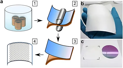
Bøggild and a team of researchers from Denmark, China, and Korea, developed a simple method for transferring A4-size sheets of CVD graphene from copper foils onto a target substrate using a commercially available polyvinyl alcohol (PVA) polymer foil as a carrier substrate and an off-the-shelf office laminator (Figure 1.1)
Figure 1.1 (a) Schematic illustration of the PVA lamination transfer process of graphene: (1) copper foils with as-grown graphene are oxidized in de-ionized water at room temperature for more than 8 hours (overnight); (2) the oxidized foils are subsequently laminated with a commercially available PVA film using a commercial hot-roll laminator. (3) After a 30-s bake on a hot plate at 110 °C, the PVA film is mechanically delaminated from the copper surface, taking the graphene film along with it (4). (b) Graphene transferred from a 10 cm × 10 cm copper foil; the dashed lines serve as a visual guide marking the edges of the graphene sheet on PVA film. (c) PVA–graphene film (from panel (b)) compared to a four-inch SiO2 on Si wafer. Reproduced from http://dx.doi.org/10.1021/acs.chemmater.8b04196 with permission from American Chemical Society, Copyright 2019.
This do-it-yourself approach requires few tools and low-cost materials—it is safe and easy enough to be carried out in school physics classes. There are no chemicals involved besides water, no spinner, and no dangerous etchants.
“PVA is widely used in industry already. It's non-toxic, biodegradable and can be washed away using only water,” says Tim Booth, an associate professor at DTU who led the work. “It's an ideal material to base an industrial process on.”
“We can transfer monolayer graphene from copper foils using a cheap office laminator in just a few minutes,” explains Abhay Shivayogimath, the paper's first author. “It is fast and easy. The best part is that we show that this method beats the two most common existing transfer methods by lengths. It is a process that anyone can learn in 20 minutes, with an equipment cost of no more than a few hundred dollars.”
The team's invention could be quite exciting for graphene producers. Now, they can supply graphene in bulk on water-soluble backing foil that customers can laminate onto their desired substrate. Customers don't need any special experience, equipment, or chemicals to complete the transfer.
The researchers note that this process can also be used to transfer other 2D materials, not just graphene, from metal surfaces.
But how about the quality? According to the team, this do-it-yourself method beats the other two dominant methods: chemical etching and bubbling transfer. Because only water is used in the whole process, there is virtually no contamination left on the graphene.
“We have shown that graphene transferred via PVA lamination has lower and more homogeneous residual doping, higher charge carrier mobility, and fewer transfer-induced defects as compared to standard chemical etching or electrochemical delamination transfers,” Shivayogimath concludes. “By avoiding any complex processing, the need for catalyst etching and recovery, and the use of organic solvents; and using only non-toxic and biodegradable materials, we have demonstrated a process which is greener, lower cost, highly scalable and more convenient for graphene growers and end-users than existing techniques, and has considerable potential for further development and use in research and industry.”
Featured scientists: Abhay Shivayogimath; Professors Peter Bøggild (https://bit.ly/2FE6xuZ) and Tim Booth
Organization: Technical University of Denmark (DTU), Lyngby (Denmark)
Relevant publication: A. Shivayogimath, P. Whelan, D. Mackenzie, B. Luo, D. Huang, D. Luo, et al., Do-It-Yourself Transfer of Large-Area Graphene Using an Office Laminator and Water, Chem. Mater., 2019, 31(7), 2328–2336.
1.3 Engineering High-tech Composite Materials
Carbon fiber-reinforced plastic (CFRP) composite materials, with their excellent strength and low specific weight properties, are suitable for all kinds of engineering applications, and they have been increasingly replacing conventional materials such as metal sheets. CFRP can be found in cars, trains, airplanes, sports equipment, windmill blades, and in many other applications where ‘lightweighting’ is an important aspect of engineering.
Of particular interest in this field are graphene-based composites. Research groups worldwide are working on the development of industrially manufacturable graphene sheets that have high strength and toughness in all sheet directions.
High-performance graphene films have many promising applications as lightweight structural materials for a variety of uses, from aircraft and automobile bodies to windmill blades and sports equipment; as flexible conductive materials for increasingly popular portable and wearable electronics; and as electromagnetic interference (EMI)-shielding materials, for eliminating the EM pollution of diverse electronic devices.
“However, improvements in mechanical and electrical properties are needed before inexpensive graphene-based composites can be used for high-performance applications,” says Qunfeng Cheng, a professor at Beihang University in Beijing. “Today, the common engineering solution is based on cross-plied carbon fibers in a polymer resin requiring high-temperature cure. In contrast, we have demonstrated cross-linked graphene sheets that are manufacturable from graphene platelets, which are re...