![]()
1
Introduction
1.1 Introduction
With the advent of nano-scale CMOS technology (sub-90nm), complex System-on-Chips (SoCs) are used in almost all the domains of electronic systems such as telecommunications, multimedia, consumer electronics, instrumentation and defense applications [24]. Despite the trend for replacement of analog functionalities within a SoC by digital signal processing operations, analog circuits are considered to be indispensable for all the applications that interface with the outer world such as interfaces with sensors, microphones, antennas, actuators, loud speakers etc. In addition, there are some mixed signal circuits, such as data converters, which contain analog components [75]. Moreover, high performance (high-speed and low power) digital circuits are often designed in an analog fashion [21].
The design complexity of an integrated circuit (IC) has increased drastically in the nano-scale domain. Several second-order effects related to nano-scale MOS transistors which were hitherto considered to be insignificant now play dominant role in determining circuit performances [66]. On the other hand, for economic reasons, the majority of the SoC application markets are characterized by shortening product life cycles and tightening time-to-market constraints. This pressure leads to the use of efficient computer-aided design (CAD) methodologies and associated design automation tools by the IC designers. In the digital domain, the design automation tools are fairly matured and commercially available. However, for analog circuits, the scenario is not so impressive [8]. Developments in the area of analog CAD tool developments are primarily in the research phase, where most of the CAD tools have been research prototypes tested on a limited set of circuits [65]. Therefore, in a complete mixed-signal integrated circuit, although analog circuits typically occupy only a small fraction of the total die area, their design is often the bottleneck, both in design time and effort [8, [66].
1.2 Characterization of Technology Scaling
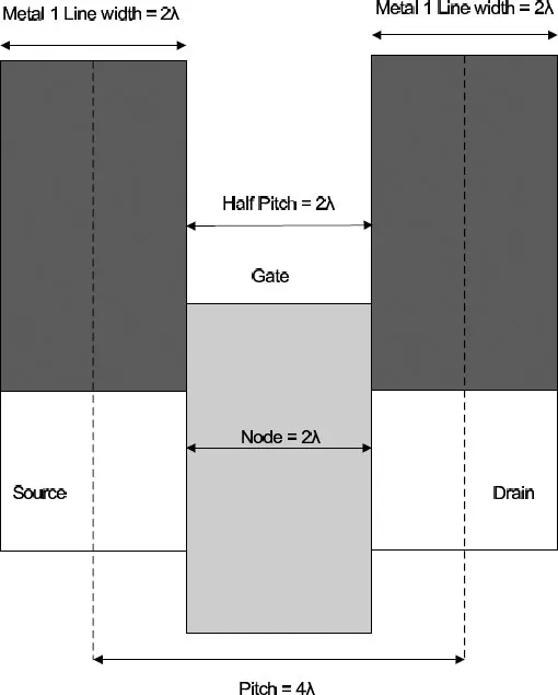
The MOS transistor feature size has been subjected to scaling down for the last few decades. The degree of scaling is measured as the half-pitch of the first-level interconnect in DRAM technology [17]. For logic circuits, the smallest feature size refers to the length of the gate of a MOS transistor. These are used to characterize a technology node. The concept of pitch and technology node are illustrated in Fig. 1.1. It is clear that half-pitch = 2 λ = technology node. Examples of technology nodes are 0.18μm, 0.13μm, 0.1μm, 90nm, 65nm, 45nm and so on. In each technology node, the feature sizes such as the contact holes in the layout of a circuit are reduced by 70% of the corresponding sizes in the earlier technology node. Consequently with each new technology generation, the circuit area is reduced by 50%, (0.7 × 0.7 = 0.49). The practice of the periodic reduction of the feature size is referred to as technology scaling. It may be noted that with advancement of CMOS device structures, the equality between the half-pitch and the technology node is violated, and today Half-Pitch > Node [91].
The most straightforward benefit of technology scaling is that with introduction of new technology the integration capacity increases twofold and thus the cost per circuit is reduced significantly. This is Gordon Moore’s law [14], according to which the complexity of MOS device integration is approximately doubled every eighteen months.
There are two major theoretical models for device scaling (i) constant field scaling and (ii) constant voltage scaling. These are discussed below
1.2.1 Constant Field Scaling
The principle of the constant field scaling is the scaling of the device voltages and dimensions (both vertical and lateral) by the same factor κ so that the electric field remains constant [43]. The doping concentration is increased by the same scaling factor κ in order to keep Poisson’s equation invariant with respect to scaling. The constant field scaling ensures that the reliability of the scaled device is not degraded compared to that of the original device.
With the scaling down of the supply voltage and transistor dimensions, a significant effect of the constant electric field scaling is that the circuit speeds up by the same factor κ and the power dissipation is reduced by κ2. In addition, the power density remains constant in the scaled transistor. The power-delay product improves by a factor κ3.
1.2.2 Constant Voltage Scaling
In spite of its significant advantages, it has been found that in reality the constant field scaling is not a feasible option. In order to keep the new devices compatible with existing components, voltages cannot be scaled arbitrarily. This necessitates multiple supply voltages which leads to considerable increase of the cost of the system. Therefore, in the constant voltage model, the voltages are kept constant [26]. The geometrical dimensions and doping, are however kept as in the case of the constant field scaling. Under the constant voltage model of scaling, the electric field is scaled up by the factor κ and the doping concentration needs to be scaled up by κ2.
FIGURE 1.1
Illustration of half-pitch and technology node.
In reality, CMOS technology evolution has followed a suitable combination of the constant field and constant voltage scaling.
1.2.3 Nonscaling Effects
In CMOS technology, the material r...