- 392 pages
- English
- ePUB (mobile friendly)
- Available on iOS & Android
eBook - ePub
VLSI Risc Architecture and Organization
About this book
With the expectation that architectural improvements will play a significant role inadvancing processor performance, it is critical for readers to maintain an up-to-date,unified overview of technological advances in this vital research area.Gathering into one place material that had been scattered throughout the literaturemakingit difficult to obtain detailed information on computer designs-this importantbook describes the main architectural and organizational features of modem mini- andmicrocomputers. In addition, it explains the RISC philosophy by supplying historicalbackground information and excellent examples of several commercially available RISCmicroprocessors.Limiting attention to VLSI implementations of RISC processors, VLSI RISCArchitecture and Organization offers insight into design issues that arose indeveloping a RISC system, using the VLSI RISC chip set developed at AcornComputers Limited as an example ... discusses options considered during the designprocess, the basis for the decisions made, and implementation details . . . describescontemporary RISC architecture, comparing and contrasting different designs ... andlooks at future trends in RISC research.Discussing the topic cohesively and comprehensively-from initial study into reducedinstructions sets to the widespread introduction of RISC architectures into mainstreamcomputer products-VLSI RISC Architecture and Organization is aninvaluable reference for electrical, electronics, and computer engineers; computerarchitects and scientists; hardware systems designers; and upper-level undergraduate andgraduate students in computer science and electrical engineering courses.
Trusted by 375,005 students
Access to over 1 million titles for a fair monthly price.
Study more efficiently using our study tools.
Information
1
The Evolution of Computer Architecture
A Reduced Instruction Set Computer (RISC) is a member of an ill-defined class of computing machines. The common factor which associates members of the class is that they all have instruction sets which have been optimized more towards implementation efficiency than members of the alternative class of Complex Instruction Set Computers (CISCs), where the optimization is towards the minimization of the semantic gap between the instruction set and a one or more high-level languages.
Though the difference in emphasis may be clear to a microprocessor designer, the resulting differences between RISC and CISC processors are often hard to identify. The introduction of the RISC approach has, however, been accompanied by a dramatic rise in the power of commercial microprocessors. For this reason it should be given a significant place in the history of architectural development.
One way to understand the significance of the RISC approach is to see it against the background of architectural development in which it first arose. In this chapter we will look at the history of computer systems, and examine some of the machines which introduced important new features that have become standard requirements on all subsequent general-purpose computers. We will also look at the underpinning technologies which are used to build computers, and see how their high rate of development is constantly shifting the ground upon which architectural decisions are based. We conclude this chapter with a description of the VAX-11/780, a very sophisticated CISC machine, and introduce by way of contrast the basis of the RISC approach.
This chapter sets the context for the RISC movement. In the second chapter we will examine the earliest RISC architectures which established the principles and formed the basis for commercial exploitation. Subsequent chapters contain descriptions of commercial designs which have to a greater or lesser extent been influenced by the RISC philosophy.
1.1 Basic Computer Architecture
A computer is a machine which performs a series of calculations on a set of numbers. The instructions for the series of calculations are called the program, the numbers are the data. A general-purpose computer is so-called because relatively few assumptions are made at the design stage about the nature of the programs which will be run on it.
The earliest general-purpose computers were mechanical, but had features which are still incorporated in their modern electronic descendants. The Babbage Analytical Engine (figure 1) was proposed in 1834, and had a memory for the data items, a central processing unit (CPU), a program using technology developed for the automatic control of weaving looms, and output to a printer or a card punch. The instruction set included branching conditionally on the sign of a number, and instructions with three operand addresses (two source and one destination). The design was never built; though technically possible, it was not well matched to the capabilities of the day.
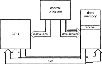
Figure 1 The Babbage Analytical Engine
1.1.1 The von Neumann Architecture
The earliest electronic machines capable of performing computations were laboriously programmed by changing the contents of a control store, in a manner analogous to changing the loom control cards in the Babbage design. The program was entirely separate from the data. A significant advance came with the removal of this separation, so that the program was kept in the same store as the data, and one program could be used to manipulate another. This stored-program concept is attributed to the designers of ENIAC, a vacuum tube based machine built for the US Army between 1943 and 1946. The concept was first expounded by von Neumann (1945), and incorporated into the IAS computer (at the Princeton Institute for Advanced Studies) which was completed in 1952. All general-purpose computers are now based on the key concepts of the von Neumann architecture (figure 2):
- A single read-write memory contains all data and instructions.
- The memory is addressable by location in a way which does not depend on the contents of the location.
- Execution proceeds using instructions from consecutive locations unless an instruction modifies this sequentiality explicitly.
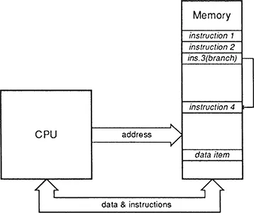
Figure 2 The von Neumann architecture
Though the von Neumann model is universal in general-purpose computing, it suffers from one obvious problem. All information (instructions and data) must flow back and forth between the processor and memory through a single channel, and this channel will have finite bandwidth. When this bandwidth is fully used the processor can go no faster. This performance limiting factor is called the von Neumann bottleneck.
1.1.2 The Harvard Architecture
A Harvard architecture (figure 3) has one memory for instructions and a second for data. The name comes from the Harvard Mark 1, an electromechanical computer which pre-dates the stored-program concept of von Neumann, as does the architecture in this form. It is still used for applications which run fixed programs, in areas such as such as digital signal processing, but not for general-purpose computing. The advantage is the increased bandwidth available due to having separate communication channels for instructions and data; the disadvantage is that the storage is allocated to code and data in a fixed ratio.
Figure 3 The Harvard architecture
Architectures with separate ports for instructions and data are often referred to by the term ‘Harvard architecture’, even though the ports connect to a common memory. For instance each port may be supplied from its own local cache memory (figure 4). The cache memories reduce the external bandwidth requirements sufficiently to allow them both to be connected to the same main memory, giving the bandwidth advantage of a Harvard architecture along with most of the flexibility of the simple von Neumann architecture. (The flexibility may be somewhat reduced because of cache consistency problems with self-modifying code.) Note that this type of Harvard architecture is still a von Neumann machine.
Although the Harvard architecture (modified or not) offers double the bandwidth of the simple von Neumann architecture, this will only allow double performance when the instruction and data traffic are equal. The VAX-11/780 has been used for a lot of measurements of memory traffic, and these measurements tend to suggest a reasonable match. RISC processors have two characteristics which make the match less good than the VAX. Firstly, they usually have less dense code, which increases the instruction traffic. Secondly, they are register to register rather than memory to memory architectures. This causes compiler writers to be much more careful about register usage, which can in turn result in much less data traffic. The use of register windows also eliminates considerable data traffic associated with procedure calls. A RISC CPU can typically require an instruction bandwidth six to ten times the data bandwidth (Patterson and Sequin, 1981), so that a Harvard architecture may only allow a ten percent speed-up (rather than the one hundred percent that would be suggested by the VAX statistics). Even so, the dual ported Harvard architecture has become a popular choice with RISC designers.
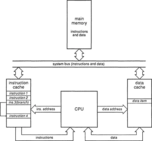
Figure 4 A modified Harvard architecture
1.1.3 The Central Processing Unit
The Central Processing Unit (CPU) of a computer is the part that executes instructions and does the computing. It consists of one or more function units, some registers, and control logic. Typically in a VLSI processor there is one function unit which is an Arithmetic and Logic Unit (ALU), though there may also be a shifter. The registers will include the user visible registers, plus others which are not visible to the user, for instance the instruction register which holds the instrucdon which is currently execudng. The control logic will be a mixture of PLAs, random logic, and possibly microcode ROM.
The part of the CPU through which data items flow is called the datapath. This includes the function units, and those registers which may contain data items. Datapaths are usually organized around buses, which are common routes for moving data from one register to another or to a functional unit. A 32-bit CPU will use 32-bit buses, so that all bits are moved simultaneously ‘in parallel’. The number of available buses is an important determinant of cost and performance. The user registers are usually arranged into a regular block (or bank) where the design of the basic cell can be highly optimized for speed and space, and the size of the cell will depend on the number of buses which run through it. For simplicity and low cost, one bus would be ideal. From the performance point of view, however, a single bus would be a severe botdeneck. A typical datapath operation reads two registers, combines them in an ALU, and writes the result back to a register, requiring three accesses in all. Normally, therefore, the register bank will have at least two read buses and one write bus. (Some designs use the same physical bus for both reading and writing.) If a CPU is to achieve a data STORE operation in a single cycle using base plus index addressing (a normal addressing mode on a CISC processor), then it must read three registers in the cycle, which requires three read buses.
Datapath design therefore usually starts from the register bank. The number and width of the registers is generally fixed in the instruction set design (though not always; see the description of the Sun SPARC in chapter 3), as are the required operations and addressing modes. If the design calls for a very high number of register bits, then the pressure to keep the the number of physical buses low is great; if the number of register bits is moderate, it may be possible to gain performance by allowing many access buses. Once the register bus structure is decided, the function units must be connected to those or other buses, and an analysis performed of the data routes required by the various instructions. The bus structure is iterated until the cost/performance balance is appropriate.
A simple CPU datapath is shown in figure 5. The register bank has two read ports which are the sources of the ALU operands, and one write port for the ALU result. The ALU result may also be written to a memory address register. For a store instruction where the address has been set up in a register, that register is placed onto the B bus and fed to the memory address register via the ALU (which is configured for this operation to feed the B bus input directly to the result), and the register to be stored is placed onto the A bus and sent to the memory. A load could use the same route to generate the address, and then feed the loaded value from memory via the A bus and ALU into the destination register.
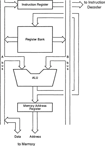
Figure 5 A simple CPU datapath
This datapath will handle internal operations and memory data accesses satisfactorily, but will be very inefficient at fetching instructions. Unless a separate instruction fetch unit is used, every new instruction will require an ALU operation to increment the program counter (which must be kept somewhere in the general register bank). If the instruction set is very complex and uses many cycles per instruction, the overhead of processing the program counter in the main ALU may be acceptable, but a RISC CPU is certain to contain some additional function unit (for instance an address incrementer) to reduce contention between the instruction fetch and execution activities.
Datapath design begins with a picture similar to this and then additional buses, registers and function units are added to avoid the bottlenecks which are identified in the course of determining the data routes for each instruction in the instruction set. It is useful to have a clear understanding of which instructions are most important to the eventual performance of the CPU, so that they are optimized in preference to less critical instructions. It is also useful to identify the theoretical minimum number of cycles for each instruction; if every memory transfer takes at least one cycle, an instruction which saves four registers will take at least four cycles, and this will usually allow considerable housekeeping activity to go on in the background at no additional cost in cycles.
Once t...
Table of contents
- Cover
- Half Title
- Title Page
- Copyright Page
- Dedication
- Table of Contents
- Preface
- 1. The Evolution Of Computer Architecture
- 2. Research Into Reduced Instruction Sets
- 3. Commercial Vlsi Risc
- 4. The Implementation of the Arm
- 5. Further Risc Research
- Acronyms
- Index
Frequently asked questions
Yes, you can cancel anytime from the Subscription tab in your account settings on the Perlego website. Your subscription will stay active until the end of your current billing period. Learn how to cancel your subscription
No, books cannot be downloaded as external files, such as PDFs, for use outside of Perlego. However, you can download books within the Perlego app for offline reading on mobile or tablet. Learn how to download books offline
Perlego offers two plans: Essential and Complete
- Essential is ideal for learners and professionals who enjoy exploring a wide range of subjects. Access the Essential Library with 800,000+ trusted titles and best-sellers across business, personal growth, and the humanities. Includes unlimited reading time and Standard Read Aloud voice.
- Complete: Perfect for advanced learners and researchers needing full, unrestricted access. Unlock 1.4M+ books across hundreds of subjects, including academic and specialized titles. The Complete Plan also includes advanced features like Premium Read Aloud and Research Assistant.
We are an online textbook subscription service, where you can get access to an entire online library for less than the price of a single book per month. With over 1 million books across 990+ topics, we’ve got you covered! Learn about our mission
Look out for the read-aloud symbol on your next book to see if you can listen to it. The read-aloud tool reads text aloud for you, highlighting the text as it is being read. You can pause it, speed it up and slow it down. Learn more about Read Aloud
Yes! You can use the Perlego app on both iOS and Android devices to read anytime, anywhere — even offline. Perfect for commutes or when you’re on the go.
Please note we cannot support devices running on iOS 13 and Android 7 or earlier. Learn more about using the app
Please note we cannot support devices running on iOS 13 and Android 7 or earlier. Learn more about using the app
Yes, you can access VLSI Risc Architecture and Organization by S.B. Furber,S. B. Furber in PDF and/or ePUB format, as well as other popular books in Computer Science & Hardware. We have over one million books available in our catalogue for you to explore.