- 544 pages
- English
- ePUB (mobile friendly)
- Available on iOS & Android
eBook - ePub
Microelectronic Materials
About this book
This practical book shows how an understanding of structure, thermodynamics, and electrical properties can explain some of the choices of materials used in microelectronics, and can assist in the design of new materials for specific applications. It emphasizes the importance of the phase chemistry of semiconductor and metal systems for ensuring the long-term stability of new devices. The book discusses single-crystal and polycrystalline silicon, aluminium- and gold-based metallisation schemes, packaging semiconductor devices, failure analysis, and the suitability of various materials for optoelectronic devices and solar cells. It has been designed for senior undergraduates, graduates, and researchers in physics, electronic engineering, and materials science.
Tools to learn more effectively

Saving Books

Keyword Search

Annotating Text

Listen to it instead
Information
1
Semiconducting Materials
1.1 INTRODUCTION
The aim of this first chapter is to introduce the basic properties of a wide range of semiconducting elements and compounds. The crystal structures and phase chemistries of semiconductors will be described first and then the structure and properties of point defects (of both intrinsic and extrinsic character) and dislocations will be presented. The role that point defects play in determining the dominant mechanism and the kinetics of the diffusion processes in semiconductors will be considered in a separate section. The emphasis of this chapter will be on presenting how the structure of, and characteristic defect concentration in, a semiconductor crystal control its electrical properties.
Here, and throughout this book, it will be assumed that the reader has a working knowledge of the simple theory of semiconductor behaviour and is familiar with the use of a one-electron diagram in describing the properties of semiconductors, defects and devices. Excellent introductions to these properties can be found in the texts by Frazer (1983) and Sze (1981).
Finally, short sections on amorphous and polymeric semiconductors are included at the end of the chapter. Some of the properties of the metallic and insulating materials used in microelectronic devices will be described in Chapters 4, 5, 6, 7.
1.2 SEMICONDUCTORS — ELEMENTS, COMPOUNDS AND ALLOYS
Many semiconductor materials have crystal structures which are related to the simple diamond cubic lattice, and a unit cell of this structure is sketched in figure 1.1(a). Each atom is tetrahedrally coordinated, but the local atomic environments are not identical for all atoms. The structure can also be thought of as consisting of two interpenetrating FCC lattices, one with origin at (0, 0, 0) and the other at . A centre of symmetry lies at the point equidistant between the origins of the two FCC lattices — at . Both silicon and germanium crystallise in this structure, and since these elements have two s and two p valence electrons it is easy to see that a full set of eight valence electrons can be gained around each atom by the promotion of one s electron to a p orbital and the formation of four covalent sp3 hybrid bonds. We shall see that most semiconductor compounds and alloys obey the principle of keeping the average electron-to-atom ratio equal to four.
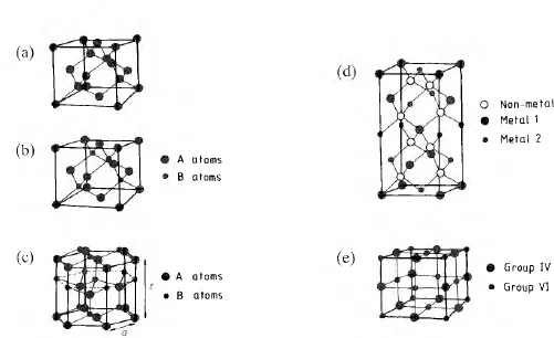
Figure 1.1 Sketches of the unit cells of semiconductor elements and compounds: (a) the diamond cubic lattice; (b) the sphalerite lattice characteristic of most III–V compounds; (c) the wurtzite lattice which can be found in some II–VI compounds; (d) the sphalerite superlattice taken up by the chalcopyrite semiconductor compounds; (e) the rocksalt crystal structure assumed by the IV–VI compounds.
The simplest illustration of this principle is given by the range of semiconductor materials AB formed between a group III element (A = B, Al, Ga and In) and one from group V (B = N, P, As and Sb). Clearly the average electron to atom ratio will be equal to four in an equiatomic compound AB. Figure 1.1(b) shows the crystal structure of one of these so-called III–V semiconductors. Let us assume that A is gallium and B is arsenic so that the compound is gallium arsenide, GaAs. The gallium and arsenic atoms occupy alternate sites in the diamond cubic lattice so that each gallium atom is surrounded by four arsenic atoms and vice versa. Crystals of this kind are often said to have the ‘zincblende’ structure because their structure is identical to that of the compound zincblende, ZnS. However, it is also called the sphalerite structure and consists of two interpenetrating FCC lattices with gallium atoms occupying one sublattice and arsenic atoms the other. All the important III–V compounds crystallise naturally with the sphalerite structure.
An interesting feature of this structure is that it has a lower symmetry than the diamond cubic lattice because there is no longer a centre of symmetry between the origins of the two FCC sublattices. This means that directions and planes with indices 111 and are not identical and each {111} surface will consist of only one kind of atom. By convention, the {111} surfaces in an AB compound are defined as containing only A atoms, while the {} surfaces contain only B atoms. The chemical properties of these two surfaces are quite different and the processes of chemical dissolution and etching proceed at different rates depending on which surface is being attacked. All crystals with the sphalerite structure show this anisotropic behaviour. In addition, these crystals show preferential cleavage on {110} planes, while diamond cubic crystals of silicon or germanium cleave more readily on {111} planes.
A second important class of compound semiconductors can be prepared by combination of a group II element (Zn, Cd and Hg) with a group VI element (S, Se and Te) to form an AB compound — the II–VI semiconductor family. Most of these compounds will crystallise with either the sphalerite or wurtzite lattice structure depending on the conditions under which the crystal is grown. A unit cell of the hexagonal wurtzite structure is sketched in figure 1.1(c). The sphalerite structure is normally the equilibrium structure at room temperature. The semiconducting properties of a II–VI semiconductor are almost independent of the crystal structure, and this can be understood when we notice that the atoms in the wurtzite lattice are tetrahedrally coordinated just as in the sphalerite lattice and the separation of nearest-neighbour atoms in the two structures is almost identical.
Another group of semiconducting materials can be formed with chemical formulae of the kind I–III–VI2 or II–IV–V2 and these compounds crystallise in a superlattice of the sphalerite structure. Some examples of the first of these kinds of compounds are AgInTe2, CuInSe2 and CuGaSe2, while ZnSiP2 and CdSiP2 are clearly II–IV–V2 compounds. The metallic sublattice in the sphalerite crystal structure is now ordered to give a unit cell like that sketched in figure 1.1(d). These ternary compound semiconductors are normally referred to as the chalcopyrites.
The III–V, II–VI and chalcopyrite semiconductor families obey the principle of having on average four valence electrons/atom, and these materials are often called ANB8–N compounds, where the superscripts are the valencies of the A and B atoms. However it is also possible to form compounds between some of the heavier group IV elements, such as Sn and Pb, and group VI chalcogenide elements like S, Se and Te. These are called the ANB10–N compounds and have an average of five valence electrons/atom. This class of materials crystallise with the rocksalt structure which is sketched in figure 1.1(e). Here each metal atom is surrounded ...
Table of contents
- Cover
- Half Title
- Title Page
- Copyright Page
- Table of Contents
- Preface
- Chapter 1 Semiconducting Materials
- Chapter 2 Contacts, Devices and Integrated Circuits
- Chapter 3 The Growth of Single Crystals of Semiconducting Materials
- Chapter 4 Polycrystalline Conducting Thin Films
- Chapter 5 The Metallurgy of Aluminium- and Gold-based Metallisation Schemes
- Chapter 6 Deposition and Properties of Insulating Films
- Chapter 7 The Packaging of Semiconductor Devices
- Chapter 8 Materials for Optoelectronic Devices
- Chapter 9 Materials for Solar Cells
- Chapter 10 Failure Analysis and the Investigation of the Structure and Composition of Microelectronic Materials
- Index
Frequently asked questions
Yes, you can cancel anytime from the Subscription tab in your account settings on the Perlego website. Your subscription will stay active until the end of your current billing period. Learn how to cancel your subscription
No, books cannot be downloaded as external files, such as PDFs, for use outside of Perlego. However, you can download books within the Perlego app for offline reading on mobile or tablet. Learn how to download books offline
Perlego offers two plans: Essential and Complete
- Essential is ideal for learners and professionals who enjoy exploring a wide range of subjects. Access the Essential Library with 800,000+ trusted titles and best-sellers across business, personal growth, and the humanities. Includes unlimited reading time and Standard Read Aloud voice.
- Complete: Perfect for advanced learners and researchers needing full, unrestricted access. Unlock 1.4M+ books across hundreds of subjects, including academic and specialized titles. The Complete Plan also includes advanced features like Premium Read Aloud and Research Assistant.
We are an online textbook subscription service, where you can get access to an entire online library for less than the price of a single book per month. With over 1 million books across 990+ topics, we’ve got you covered! Learn about our mission
Look out for the read-aloud symbol on your next book to see if you can listen to it. The read-aloud tool reads text aloud for you, highlighting the text as it is being read. You can pause it, speed it up and slow it down. Learn more about Read Aloud
Yes! You can use the Perlego app on both iOS and Android devices to read anytime, anywhere — even offline. Perfect for commutes or when you’re on the go.
Please note we cannot support devices running on iOS 13 and Android 7 or earlier. Learn more about using the app
Please note we cannot support devices running on iOS 13 and Android 7 or earlier. Learn more about using the app
Yes, you can access Microelectronic Materials by C.R.M. Grovenor in PDF and/or ePUB format, as well as other popular books in Physical Sciences & Physics. We have over one million books available in our catalogue for you to explore.