Two-dimensional (2D) materials have attracted tremendous interest since the study of graphene in the early 21st century. With their thickness in the angstrom-to-nanometer range, 2D materials, including graphene, transition metal dichalcogenides, phosphorene, silicene, and other inorganic and organic materials, can be an ideal platform to study fundamental many-body interactions because of reduced screening and can also be further engineered for nanophotonic applications.
This book compiles research outcomes of leading groups in the field of 2D materials for nanophotonic physics and devices. It describes research advances of 2D materials for various nanophotonic applications, including ultrafast lasers, atomically thin optical lenses, and gratings to inelastically manipulate light propagation, their integrations with photonic nanostructures, and light–matter interactions. The book focuses on actual applications, while digging into the physics underneath. It targets advanced undergraduate- and graduate-level students of nanotechnology and researchers in nanotechnology, physics, and chemistry, especially those with an interest in 2D materials.
An Introduction of 2D Materials for Nanophotonic Devices
Jiong Yanga,b and Yuerui Lua,c
a College of Chemistry and Environmental Engineering, Shenzhen University, Shenzhen 518060, China
b Key Laboratory of Optoelectronic Devices and Systems of Ministry of Education and Guangdong Province, College of Optoelectronic Engineering, Shenzhen University, Shenzhen 518060, China
c Research School of Engineering, College of Engineering and Computer Science, Australian National University, Canberra ACT 2601, Australia [email protected]; [email protected]
In 1704, Sir Isaac Newton demonstrated with a prism that white light could be resolved into its component colours and would form a rainbow, and then he refracted the resolved spectrum back together with a second prism, proving that prisms would not colour light [1]. Now we know that white light is composed of lights of different frequencies, and they will be refracted to different angles when interacting with a prism. light–matter interactions can be classified into inelastic and elastic interactions [2]. Inelastic interactions involve energy transfer between photons and electrons or phonons. Photon–electron and photon–phonon interactions will result in photo-luminescence (PL) phenomenon and the Raman effect, respectively. By using PL and Raman spectroscopy to characterise 2D semiconductors, their intrinsic properties can be well understood, including the optical bandgap [3], carrier recombination mechanism [4], atomic bonds and thermal properties [5, 6]. In contrast, elastic interactions do not involve energy transfer and are responsible for controlling light propagation. Optical components, from conventional cavities [7], waveguides [8], lenses [9] and gratings [10] to recent optical meta-materials [11] and photonic crystals [12], all rely on strong elastic light–matter interactions to achieve sophisticated control of light propagation.
Two-dimensional materials are a family of crystalline materials consisting of a single layer or a few layers of atoms, including zero-bandgap graphene [13, 14], middle-bandgap transition metal dichalcogenide (TMD) and phosphorene [15, 16] and wide-bandgap hexagonal boron nitride (hBN) [17]. They own unique properties originated from their large surface-to-volume ratio and reduced dielectric screening [18, 19, 20, 21, 22, 23, 24, 25]. And plenty of research has been conducted to investigate their thermal, electrical, optical and optoelectronic properties [15, 26, 27, 28, 29, 30]. Among those distinct characteristics, optical properties of 2D semiconductors are especially intriguing and much efforts have been drawn to this field, including Raman and PL spectroscopic analysis [5, 6, 29, 31], exciton (a quasi-particle consisting of one electron and one hole), trion (charged exciton) and higher-order complex study [32, 33, 34, 35], refractive index measurement [36, 37, 38, 39] and investigation of light–matter interactions [40, 41, 42, 43, 44, 45, 46].
light–matter interactions of 2D materials can be further modified by directly processing them into specific shapes [45, 47, 48, 49] or by coupling them with artificial nanostructures [50, 51, 52], and thus nanophotonic devices based on 2D materials can be fabricated. By using laser micro-/nanomanufacturing and the photo-chemical reaction technique, Lu et al. fabricated thin-layer TMDs and black phosphorus (BP) colour-sensitive structures [53, 54]. And by using gallium ion beam to mill thin-layer MoS2 into certain shapes, Yang et al. successfully fabricated atomically thin optical lenses and gratings to modify light propagation [49]. Besides, Li et al. have successfully observed pulse generation from graphene and BP [55, 56, 57]. In addition to the aforementioned nanophotonic devices based on 2D materials, researchers have coupled 2D materials with plasmonic, photonic and other on-chip devices to demonstrate other applications, including second harmonic generation (SHG) enhancement and light-emitting devices [58, 59, 60].
In this book, research groups around the world working on light–matter interactions of 2D semiconductors will conclude their recent research progress, including optical property characterisation of 2D semiconductors, and ultra-fast lasers, non-linear optical devices, photonic crystals, plasmonic cavities and micro-lens and gratings fabricated from 2D semiconductors and their performance characterisation.
1.1 Two-Dimensional Semiconductors
In this section, we will briefly introduce recent research advances of several typical 2D semiconductors, including graphene, transition metal dichalcogenides (TMDs) and phosphorene. Graphene has been most widely studied as a 2D zero-bandgap semiconductor since its first demonstration by Novoselov and Geim et al. [61]. Later, TMD semiconductors rise up due to their intrinsic bandgap and the direct-bandgap nature when thinning down to a single layer [15, 62]. And recently, phosphorene has attracted much attention because of its highly anisotropic nature and direct bandgap in the infrared range [63]. In this section, we will briefly introduce the physical, electrical and optical properties of those 2D semiconductors.
1.1.1 Graphene
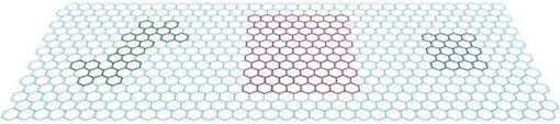
Graphene has been most widely studied in the family of 2D materials because of its high mobility, optical transparency, flexibility, robustness and environmental stability, making it a promising candidate for fundamental research and electrical, optical and optoelectronic applications [64]. Graphene is a flat single layer (or a few layers) of carbon atoms that are tightly packed into a 2D hexagonal honeycomb lattice, and its schematic plot is shown in Fig. 1.1. Graphene is well known for its large intrinsic strength predicted to exceed that of any other materials [65], huge thermal conductivity of ~5000 W/mK at room temperature [27] and gate-tunable high electric conductivity [14].
Figure 1.1 Schematic plot of graphene. Reprinted with permission from Springer Customer Service Centre GmbH: Springer Nature, Nature Materials, Ref. [13], Copyright (2007).
Lee et al. measured the elastic properties and intrinsic strength of monolayer (1L) graphene by nanoindentation in atomic force microscopy (AFM) [65]. The measured second- and third-order elastic stiffness is 340 Nm−1 and −690 Nm−1, respectively. The measured effective Young’s modulus is about 1 TPa, and the measured effective pre-stress and pre-tension can reach ~0.7 GPa and 0.4 ...
Table of contents
Cover
Half Title
Title Page
Copyright Page
Table of Contents
Preface
1. An Introduction of 2D Materials for Nanophotonic Devices
2. light–matter Interactions in 2D Materials
3. Atomically Thin Optical Lenses and Gratings
4. Two-Dimensional Layered Materials for Optical Pulse Generation
5. Plasmonic-Nanostructure-Enhanced Optical Properties of 2D Materials
6. Integration of 2D Materials with Photonic Nanostructures
7. Strong light–matter Interactions in 2D Materials Assisted by On-chip Optoelectronic Devices
Index
Frequently asked questions
Yes, you can cancel anytime from the Subscription tab in your account settings on the Perlego website. Your subscription will stay active until the end of your current billing period. Learn how to cancel your subscription
No, books cannot be downloaded as external files, such as PDFs, for use outside of Perlego. However, you can download books within the Perlego app for offline reading on mobile or tablet. Learn how to download books offline
Perlego offers two plans: Essential and Complete
Essential is ideal for learners and professionals who enjoy exploring a wide range of subjects. Access the Essential Library with 800,000+ trusted titles and best-sellers across business, personal growth, and the humanities. Includes unlimited reading time and Standard Read Aloud voice.
Complete: Perfect for advanced learners and researchers needing full, unrestricted access. Unlock 1.4M+ books across hundreds of subjects, including academic and specialized titles. The Complete Plan also includes advanced features like Premium Read Aloud and Research Assistant.
Both plans are available with monthly, semester, or annual billing cycles.
We are an online textbook subscription service, where you can get access to an entire online library for less than the price of a single book per month. With over 1 million books across 990+ topics, we’ve got you covered! Learn about our mission
Look out for the read-aloud symbol on your next book to see if you can listen to it. The read-aloud tool reads text aloud for you, highlighting the text as it is being read. You can pause it, speed it up and slow it down. Learn more about Read Aloud
Yes! You can use the Perlego app on both iOS and Android devices to read anytime, anywhere — even offline. Perfect for commutes or when you’re on the go. Please note we cannot support devices running on iOS 13 and Android 7 or earlier. Learn more about using the app
Yes, you can access Two-Dimensional Materials in Nanophotonics by Yuerui Lu in PDF and/or ePUB format, as well as other popular books in Computer Science & Optical Data Processing. We have over one million books available in our catalogue for you to explore.