1.1 Introduction
Due to the limited availability and relatively high cost of sufficiently large GaN substrates for homoepitaxial growth, GaN films are normally grown on foreign substrates, such as sapphire, SiC, and Si. Table 1.1 shows properties of III nitrides and these foreign substrates. SiC has the smallest lattice mismatch and thermal expansion coefficient (TEC) mismatch to GaN as compared to others, but the high price and limited diameter (normally ≤6 inches) of a SiC substrate make it unaffordable for power applications. GaN-on-sapphire substrate technology is very mature and is the mainstream in the light-emitting diode (LED) market, but it is unsuitable for power applications due to the poor thermal conductivity of sapphire.
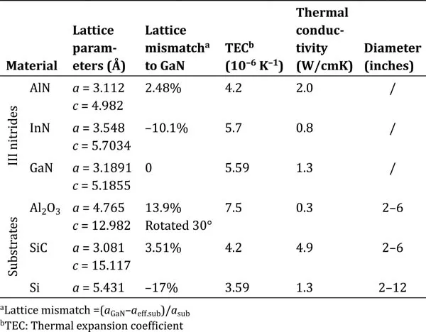
Si is the most widely used semiconductor nowadays, and using a Si substrate has many advantages over SiC and sapphire, such as a large diameter, low cost, and a ready-made process. The diameter of a Si substrate can be scaled to 12 inches, and the metal-organic chemical vapor deposition (MOCVD) reactor is available to grow 8-inch GaN epilayers on 8-inch Si substrates. In contrast, the SiC and sapphire substrate size is typically smaller than 6 inches. The cost of GaN power devices can be further reduced by using the ready-made 6- and 8-inch complementary metal-oxide-semiconductor (CMOS) process line. A Si substrate also shows high crystalline quality and minimized defect density, thanks to decades of development of the Si semiconductor industry. It has been well accepted that GaN on large-size silicon substrates is one cost-effective way to achieve high-volume production of GaN power devices. Figure 1.1 shows the epitaxial relationship of the GaN(0001) plane (c-plane) on the Si(111) plane. Usually, a Si(111) substrate is utilized for the epitaxial growth of c-plane GaN because of their same trigonal symmetry.
Table 1.1 Properties of III nitrides and substrates [1, 2]
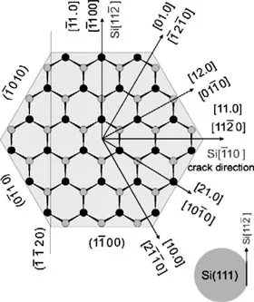
However, the growth of GaN on Si is challenging owing to issues such as melt-back etching and a large thermal and lattice mismatch [4]. A common problem in the growth of GaN on Si is melt-back etching. The origin of melt-back etching is the alloying reaction between Ga and Si at high temperature (HT). Ga has high solubility in Si at high temperature. When Ga comes in contact with Si at high temperature, the alloy of Ga and Si forms and produces hollows and swellings on the substrate, which seriously destroys the epilayers (Fig. 1.2). Once the melt-back-etching process starts, it will expand during the following growth and cannot be stopped. Therefore it is extremely important to prevent melt-back for growing GaN on Si. Ga-free layers, such as AlN, SiC [5], AlAs [6], and Al2O3 [7], were employed to prevent Ga from contacting Si. Ascribed with the advantages of high thermal stability and convenience, AlN is normally used as a starting buffer layer for GaN on Si.
Figure 1.1 Epitaxial relationship GaN(0001) on Si(111). Reprinted from Ref. [3], Copyright (2002), with permission from Elsevier.
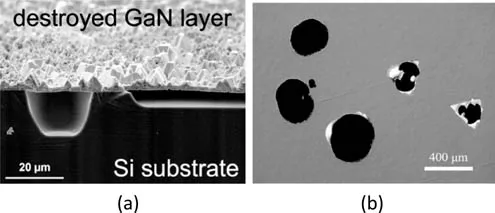
One of the biggest challenges is the large stress caused by the thermal mismatch between GaN epilayers and Si substrates. The TEC of GaN is 5.59 × 10⁻⁶ K–1, which is much larger than that of Si, 3.59 × 10⁻⁶ K–1. A GaN epilayer is usually grown at a high temperature of 1000°C using MOCVD. When GaN is cooling down from growth temperature to room temperature, a large tensile stress of about 1 Gpa is generated in the GaN film because the TEC of the Si substrate is significantly smaller than that of GaN. Consequently, there is a much greater risk that the GaN epilayers will crack if the thickness of GaN exceeds several hundred nanometers, as shown in Fig. 1.3. A GaN layer with a thickness of several hundred nanometers is insufficient for producing high-quality films and devices. GaN electronics on Si can easily break down from the Si substrate because of the low critical electric field of Si. To achieve a high breakdown voltage, a film thickness of several micrometers is necessary for a GaN-on-Si power device.
Figure 1.2 Destroyed GaN layer due to melt-back etching: (a) SEM image of a vertical view. Reprinted from Ref. [8], Copyright (2003), with permission from Elsevier. (b) Optical microscope image of a plan view.
Stress also introduces large wafer bow, which deteriorates the uniformity of the epilayer and causes failure during wafer handling and passing of the stepper in the lithography process, making the material unsuitable for device manufacturing. The wafer curvature k can be obtained from the Stoney equation:
where εm, Mf, Ms, hf, and hs denote the biaxial mismatch strain, the biaxial moduli of the film, the biaxial moduli of the substrate, the thickness of the film, and the thickness of the substrate, respectively. Assuming the diameter of the substrate is D, the wafer bow can be obtained by
The wafer bow is proportional to the square of the substrate diameter, indicating a larger value when a large-diameter Si substrate is utilized.
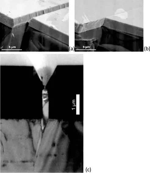
To grow crack-free GaN on Si with low wafer bow, stress engineering has to be executed. Compressive stress is introduced during growth by inserting Al-rich layers such as AlN [9,10,11,12 and 13], AlGaN [14,15,16,17,18,19,20,21,22,23 and 24], and AlN/GaN superlattices (SLs) [25,26,27,28 and 29] to counterbalance the tensile stress. Nevertheless, this compressive stress also should be carefully controlled. This compressive stress causes curvature of the wafer during growth, which will deteriorate the wafer temperature uniformity and cause plastic deformation (Fig. 1.4) if a too large curvature appears [30]. Thus stress engineering is of great importance and is challenging for the growth of a GaN-on-Si wafer.
Figure 1.3 Two types of cracks for GaN on Si: (a) an open groove with facets occurs during growth and (b) a closed crack during cooling down; (c) cross section of an open crack. Reprinted from Ref. [3], Copyright (2002), with permission from Elsevier.
The large lattice mismatch between GaN and Si will introduce a high density of dislocations, which are usually larger than 108/cm2. High dislocation densities deteriorate the crystalline quality of GaN and the performance of power devices.
Apart from the large tensile stress and high dislocation density, GaN on Si has also suffered from high buffer leakage, which should be minimized for power applications. Compared to Si and GaAs, GaN grown on a heterosubstrate is a very imperfect crystal system with a high density of defects. Usually, the density of the background donor in unintentionally doped GaN is 1016–1017/cm3 due to the existence of oxygen and silicon impurities and nitrogen vacancies, which introduces 1016–1017/cm3 ba...