Extending Moore's Law through Advanced Semiconductor Design and Processing Techniques
- 354 pages
- English
- ePUB (mobile friendly)
- Available on iOS & Android
Extending Moore's Law through Advanced Semiconductor Design and Processing Techniques
About this book
This book provides a methodological understanding of the theoretical and technical limitations to the longevity of Moore's law. The book presents research on factors that have significant impact on the future of Moore's law and those factors believed to sustain the trend of the last five decades. Research findings show that boundaries of Moore's law primarily include physical restrictions of scaling electronic components to levels beyond that of ordinary manufacturing principles and approaching the bounds of physics. The research presented in this book provides essential background and knowledge to grasp the following principles:
- Traditional and modern photolithography, the primary limiting factor of Moore's law
- Innovations in semiconductor manufacturing that makes current generation CMOS processing possible
- Multi-disciplinary technologies that could drive Moore's law forward significantly
- Design principles for microelectronic circuits and components that take advantage of technology miniaturization
- The semiconductor industry economic market trends and technical driving factors
The complexity and cost associated with technology scaling have compelled researchers in the disciplines of engineering and physics to optimize previous generation nodes to improve system-on-chip performance. This is especially relevant to participate in the increased attractiveness of the Internet of Things (IoT). This book additionally provides scholarly and practical examples of principles in microelectronic circuit design and layout to mitigate technology limits of previous generation nodes. Readers are encouraged to intellectually apply the knowledge derived from this book to further research and innovation in prolonging Moore's law and associated principles.
Tools to learn more effectively

Saving Books

Keyword Search

Annotating Text

Listen to it instead
Information
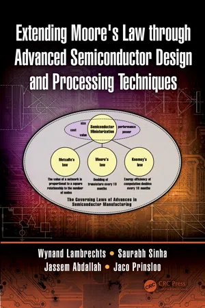
1 | The Driving Forces Behind Moore’s Law and Its Impact on Technology |
Scaling Results for Circuit Performance
| Component or IC Parameter | Scaling Factor |
| Physical device dimensions (t ox , L, W) | 1/κ |
| Doping concentration (N A ) | κ |
| Operating voltage (V) | 1/κ |
| Circuit current (I) | 1/κ |
| Capacitance (C) | 1/κ |
| Delay time per circuit (VC/I) | 1/κ |
| Power dissipation per circuit (VI) | 1/κ 2 |
| Power density ( VI / A ) | κ |
| (1.1a) |
f | is the operating frequency in Hz |
C | is the component capacitance and V is the operating (bias) voltage |
| (1.1b) |
| (1.2) |
P ds | is the dynamic switching power dissipation as a function of the operating frequency and charging and discharging through capacitances |
P sc | is the short-circuit power dissipation |
P sb | is the static biasing power dissipation due to the direct current (DC) consumed by the active device under its DC operating conditions, which include P leakage |
Table of contents
- Cover
- Half-Title
- Title
- Copyright
- Authors
- Contents
- Chapter 1 The Driving Forces Behind Moore’s Law and Its Impact on Technology
- Chapter 2 The Economics of Semiconductor Scaling
- Chapter 3 The Importance of Photolithography for Moore’s Law
- Chapter 4 Photolithography Enhancements
- Chapter 5 Future Semiconductor Devices
- Chapter 6 Microelectronic Circuit Thermal Constrictions Resulting from Moore’s Law
- Chapter 7 Microelectronic Circuit Enhancements and Design Methodologies to Facilitate Moore’s Law – Part I
- Chapter 8 Microelectronic Circuit Enhancements and Design Methodologies to Facilitate Moore’s Law – Part II
- Chapter 9 The Evolving and Expanding Synergy Between Moore’s Law and the Internet-of-Things
- Chapter 10 Case Studies
- Index
Frequently asked questions
- Essential is ideal for learners and professionals who enjoy exploring a wide range of subjects. Access the Essential Library with 800,000+ trusted titles and best-sellers across business, personal growth, and the humanities. Includes unlimited reading time and Standard Read Aloud voice.
- Complete: Perfect for advanced learners and researchers needing full, unrestricted access. Unlock 1.4M+ books across hundreds of subjects, including academic and specialized titles. The Complete Plan also includes advanced features like Premium Read Aloud and Research Assistant.
Please note we cannot support devices running on iOS 13 and Android 7 or earlier. Learn more about using the app