- 424 pages
- English
- ePUB (mobile friendly)
- Available on iOS & Android
eBook - ePub
VLSI Design
About this book
Very Large Scale Integration (VLSI) has become a necessity rather than a specialization for electrical and computer engineers. This unique text provides Engineering and Computer Science students with a comprehensive study of the subject, covering VLSI from basic design techniques to working principles of physical design automation tools to leading edge application-specific array processors.
Beginning with CMOS design, the author describes VLSI design from the viewpoint of a digital circuit engineer. He develops physical pictures for CMOS circuits and demonstrates the top-down design methodology using two design projects - a microprocessor and a field programmable gate array. The author then discusses VLSI testing and dedicates an entire chapter to the working principles, strengths, and weaknesses of ubiquitous physical design tools. Finally, he unveils the frontiers of VLSI. He emphasizes its use as a tool to develop innovative algorithms and architecture to solve previously intractable problems.
VLSI Design answers not only the question of "what is VLSI," but also shows how to use VLSI. It provides graduate and upper level undergraduate students with a complete and congregated view of VLSI engineering.
Tools to learn more effectively

Saving Books

Keyword Search

Annotating Text

Listen to it instead
Information
Subtopic
ComputertechnikChapter 1 Introduction
The story begins...
Our story began in 1948 when William Shockley, John Bardeen, and Walter H. Brattain of Bell Laboratories invented the transistor. Currently, a majority of integrated circuits are built with a type of transistor called the metal-oxide-semiconductor field-effect transistor (MOSFET).
An integrated circuit (IC) is a tiny semiconductor chip, on which a complex of electronic components and their interconnections are fabricated with a set of pattern defining masks.1 The technique of fabricating an IC with a set of masks is somewhat analogous to that of creating a photograph with a negative. We describe a typical IC fabrication process in Chapter 3.
The concept of fabricating multiple electronic devices and their interconnections entirely on a small semiconductor chip was proposed shortly after the transistor was invented. ICs began to become commercially available in the early 1960s. IC design and fabrication technologies have been developed at a phenomenal rate since then.
The evolution of IC technology is measured by the number of components integrated on a single chip. The IC industry has gone through the milestones of small scale integration (SSI), medium scale integration (MSI), large scale integration (LSI), and very large scale integration (VLSI).
Fig. 1.1 shows the approximate number of transistors available on a single chip in each of these periods.
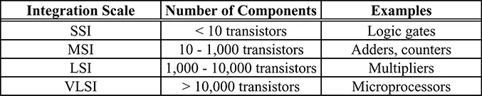
Fig. 1.1 Integration scales.
In 1965, Gordon Moore (a cofounder of Intel) made an observation and prediction on the development of semiconductor technology. His prediction is that the effectiveness of semiconductor technology, as roughly measured by the maximum number of transistors on a chip, approximately doubles every eighteen months. This forecast, now commonly known as “Moore’s law,” has been accurate for the last four decades. A depiction of Moore’s law is shown in Fig. 1.2. Note that the y-axis is drawn in a logarithmic scale. The rapid advance of IC technology is evident from the fact that the on-chip transistor count has increased one million times in three decades.
1 Both terms “integrated circuit” and “chip” will be used interchangeably in this book.
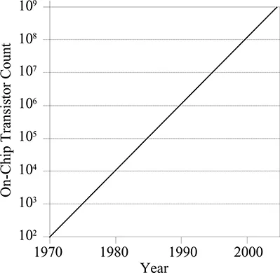
Fig. 1.2 Moore’s law.
The exponential growth of IC technology is also evident in the smallest manufacturable feature size (minimum line width), which has been reduced from around 10 μm in the 1970s to less than 0.2 μm in 2000 and continues to decrease. One micrometer (μm), also called a micron, equals 1 × 10⁻⁶ m and is commonly used as the basic length unit in IC design. The use of an even smaller length unit, the nanometer (nm), is getting increasingly popular. One μm equals 1000 nm. Physicists predict that the lower bound of feature size is around 0.05 μm (50 nm) for the current form of MOSFET ICs.
While Fig. 1.1 shows that any circuits with more than 10,000 transistors are considered to be in the VLSI category, currently millions of transistors are routinely integrated into a single chip. For example, the Intel Pentium III processor has 28 million transistors and is fabricated with a technology that provides a minimum feature size of 0.18 μm. It operates at 700 MHz and performs 2000 million instructions per second (MIPS).
The creation of a VLSI circuit involves a large number of activities such as logic design, modeling, simulation, testing, and fabrication, each of which can in turn be divided into many tasks. A broad spectrum of knowledge ranging from solid state physics to logic circuit design is required to successfully carry out all these steps. The rapid advancement of manufacturing capability has apparently enabled the growth of integration density. However, without the methodology specifically developed for the design of VLSI circuits, the potential of advanced manufacturing techniques would not have been realized. We will describe the VLSI design methodology in the next section.
1.1 VLSI Design Methodology
The VLSI design methodology developed by Mead and Conway and others in the late 1970s released the IC designers from the details of semiconductor manufacturing, so they could concentrate their efforts on coping with the circuit functionality.2 This design methodology, illustrated in Fig. 1.3 as an exchange of information between the IC designers (design team) and semiconductor engineers (silicon foundry), is largely responsible for the success of the IC industry in the last two decades. The third participant of the IC industry is the computer-aided design (CAD) tool providers who develop software tools to support design activities. Fig. 1.3 also shows that CAD tool providers often optimize their tools for specific fabrication processes.
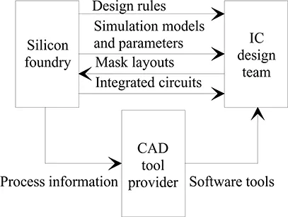
Fig. 1.3 Relationship between a silicon foundry, an IC design team, and a CAD tool provider.
Fig. 1.3 shows that the design and fabrication of an IC are typically performed by two separate teams with different expertise — a silicon foundry (an IC manufacturer that provides fabrication services to clients) and an IC design team. A silicon foundry develops and provides design rules compatible with its fabrication technology to its clients. Design rules are a set of dimensional rules (e.g., minimum line widths, minimum spacings, etc.) determined by considering the physical limitations of a fabrication process. Furthermore, simulation models of the active and passive devices fabricated by a certain process are developed and made available to the logic designers.
2 C. A. Mead and L. A. Conway, Introduction to VLSI Systems, Addison-Wesley, 1980.
The IC designers use CAD tools to create mask layouts which represent how components and connections should be formed on a semiconductor wafer. These designs, after being simulated and verified, are delivered to the silicon foundry, which produces ICs according to these mask layouts.
The chance of successfully fabricating a chip design that conforms to the design rules is very high. However, the reader should realize that a successfully processed chip is not necessarily equivalent to a functionally correct one. The principle of “garbage in, garbage out” applies. The function and performance of a chip can be predicted by simulation with reasonable accuracy.
The most important design principle emphasized in the VLSI design methodology is to divide-and-conquer. Instead of dealing with an entire VLSI circuit altogether at the same time, the designer partitions it into smaller and thus more manageable parts. These parts may further be broken down into even smaller building blocks. The partitioning of a VLSI system into increasingly smaller subsystems so that they can be handled efficiently is called the hierarchical design methodology. CAD tools have been developed to automate the steps in a hierarchical design.
In this chapter, we provide a general overview of the VLSI design process. It is the intention of the chapter to provide the reader with a qualitative understanding of the steps involved in the VLSI design process. The details of these steps are explained and discussed in later chapters.
1.2 VLSI Design — An Overview
The time will come when we want to discuss the process of designing sophisticated VLSI systems. At this moment, we need a representative, yet relatively simple circuit to demonstrate a typical design process. The design of an arithmetic adder is selected here for this purpose. The reader should notice the similarities and differences between the design of a VLSI chip and a printed circuit board system.
Technology
It is reasonable to assume that a design should begin by studying the characteristics of available fabrication processes. This overview thus begins with an introduction to the IC fabrication technology. However, as explained in the last section, the modern IC design methodology separates the designers from the semiconductor processing tasks so there is no urgent need to select a specific IC fabrication technology at the initial phase of the design. A general knowledge of the fabrication process is sufficient at this point.
The major materials that are used to build semiconduc...
Table of contents
- Cover Page
- Title Page
- Copyright Page
- Contents
- PREFACE
- 1 INTRODUCTION
- 2 CMOS LOGIC CIRCUITS
- 3 IC LAYOUT AND FABRICATION
- 4 CMOS CIRCUIT CHARACTERIZATION
- 5 SEQUENTIAL LOGIC CIRCUITS
- 6 ALTERNATIVE LOGIC STRUCTURES
- 7 SUB-SYSTEM DESIGN
- 8 CHIP DESIGN
- 9 TESTING
- 10 PHYSICAL DESIGN AUTOMATION
- 11 PARALLEL STRUCTURES
- 12 ARRAY PROCESSORS
- 13 FAULT TOLERANT VLSI ARCHITECTURES
- INDEX
Frequently asked questions
Yes, you can cancel anytime from the Subscription tab in your account settings on the Perlego website. Your subscription will stay active until the end of your current billing period. Learn how to cancel your subscription
No, books cannot be downloaded as external files, such as PDFs, for use outside of Perlego. However, you can download books within the Perlego app for offline reading on mobile or tablet. Learn how to download books offline
Perlego offers two plans: Essential and Complete
- Essential is ideal for learners and professionals who enjoy exploring a wide range of subjects. Access the Essential Library with 800,000+ trusted titles and best-sellers across business, personal growth, and the humanities. Includes unlimited reading time and Standard Read Aloud voice.
- Complete: Perfect for advanced learners and researchers needing full, unrestricted access. Unlock 1.4M+ books across hundreds of subjects, including academic and specialized titles. The Complete Plan also includes advanced features like Premium Read Aloud and Research Assistant.
We are an online textbook subscription service, where you can get access to an entire online library for less than the price of a single book per month. With over 1 million books across 990+ topics, we’ve got you covered! Learn about our mission
Look out for the read-aloud symbol on your next book to see if you can listen to it. The read-aloud tool reads text aloud for you, highlighting the text as it is being read. You can pause it, speed it up and slow it down. Learn more about Read Aloud
Yes! You can use the Perlego app on both iOS and Android devices to read anytime, anywhere — even offline. Perfect for commutes or when you’re on the go.
Please note we cannot support devices running on iOS 13 and Android 7 or earlier. Learn more about using the app
Please note we cannot support devices running on iOS 13 and Android 7 or earlier. Learn more about using the app
Yes, you can access VLSI Design by M. Michael Vai in PDF and/or ePUB format, as well as other popular books in Technik & Maschinenbau & Computertechnik. We have over one million books available in our catalogue for you to explore.