The emergence and rapid growth of the microelectronic industry, and its concomitant drive for the miniaturization of electronic devices, together with the optical fiber telecommunication industry and its need to couple light in and out of single mode waveguides, has created in their wake, a new area of optics termed “micro-optics”. What is meant by this term is optical elements of dimension of a millimeter or smaller. Primarily, this has meant lenses, or elements that act as lenses, as well as structures that redirect, polarize, and otherwise alter some state or direction of light. These would include elements like, mirrors, gratings, polarizers, and the like, made in some “micro” form. If one includes optical wave-guide structures as well, this broader classification can be considered under the name, “integrated optics”. Another interesting aspect of the evolution of micro-optics has been, not only has the microelectronic industry supplied the need for tiny optical devices, but has been able, in some cases, to supply the technology by which it can be fabricated. We will see in a later chapter that the very microfabrication technology used to fabricate microcircuits can be used to produce patterns that provide optical function through diffraction of light. This is but one way in which small optical elements, primarily lenses and lens arrays can be fabricated.
One can find discussions of devices that contain micro-optic elements, often done in a comprehensive, but narrow way [1]. However, here the device and its performance are stressed, and the elements themselves are not discussed in any real detail. Moreover, the possible alternative methods are not compared and discussed. There are monographs dealing with particular technologies, like gradient index, and consequently they do not deal with the alternatives [2]. There are a few encyclopedic-type publications that discuss optical elements, but never deal with the optical elements and the methods of fabrication in any detail [3,4]. In this book we try to stress the optical elements and how they are fabricated as well as try to give sufficient applications where the reader can appreciate the interplay and implications of a particular approach. We will attempt to address some of these fabrication and application methods in some detail. In addition, we will introduce some of the new micro-optic phenomena that may find its way into applications in the near future.
The exposition will be broken down into four parts. In the first part, we will deal with the important optical element called the “microlens”. These microlenses are found in numerous optical devices and therefore will be given significant attention. Chapters 2–4 will deal with the different ways that microlenses can be fabricated along with a brief review of the underlying optic principles, Here, we will emphasize the properties and fabrication methods.
The structure of the first part of the book will be to separate the lens fabrication techniques into the type of lens. For example, the categories refractive lenses, gradient index lenses, and diffractive lenses will constitute individual chapters. For each of these lens types, we will give a brief optics background, sufficient for the reader to appreciate the advantages, limitations, and problems that subsequently arise as a consequence of the optical imaging principles. This is particularly important when one is trying to compare, say, the efficiency of a gradient index lens to a diffractive lens. Although the function is the same, to gather light from an object and direct it to an image, the formulation of the imaging is done in a different way, thus the reader must be familiar with at least, the terminology, if not the optical principles. Under each lens category, we will further discuss the various fabrication methods. For example, under the refractive lens heading, we will discuss methods such as molded, photosensitive glass, etching, etc. The advantages and disadvantages of the fabrication method will be discussed. Because many of these fabrication methods are the property of commercial companies, we will give the general approach to the fabrication rather than a recipe. Where we can, we will refer specifically to the commercial vendors.
In the next part, Chapters 5 and 6, we will deal with the variety of application of microlens arrays. We will cover the one-to-one imaging application of lens arrays in Chapters 5. The major applications will be as lens bars for scanning and reading documents. In Chapters 6, we will cover the wide range of two-dimensional lens arrays that find application in many diverse areas. In these two chapters, it will become clear the distinction in applications where the arrays are used to image collectively, that is act like a conventional larger lens, and those where each microlens acts independently. In the fabrication of a microlens array, in addition to the attention that must be paid to develop the properties of individual lens itself, equal attention must be paid to the manner in which exact positioning of the lenses relative to some fixed point can be accomplished. In a single lens, one can imagine a mounting fixture that permits the accurate positioning of the lens relative to the light source, or fiber. However, if a lens array is to be aligned to, for example, a laser diode array with a well-specified center-to-center distance as a consequence of its fabrication, alignment may never be possible, if the spacing between the lenses was not maintained during its fabrication. One is dealing with maintaining alignment of microns over centimeters. This adherence to dimensional stability over dimensions of many centimeters can make the defining difference in the choice of what method to use for any given application. This adds another aspect to the manufacture of lens arrays which brings in the temperature of the process and how it affects the geometric stability of the substrate. Since some common substrate materials, in particular glass, undergo some degree of irreversible volume change upon heating, the extent of which depends on the temperature relative to the fictive temperature, the maximum temperature achieved during the fabrication can be critical. Because of this more critical requirement, we will be mainly dealing in this book with the methods by which lens arrays are made.
Because the impetus for micro-optic elements has come simultaneously from two different directions, microelectronics and optical telecommunications, the optical lens design and performance as well as the size and layout are different enough to influence the optimum fabrication method. This will be made clear in the subsequent discussions of the individual fabrication techniques as they relate to applications. Consider the following areas that have been of interest over the past few years.
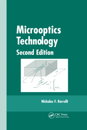
Compact optical devices requiring imaging optics to be confined to a small space. Examples of this are document readers, bar code readers, and scanners. These particular applications require erect one-to-one imaging. The advantage of using a lens bar-shaped lens array for essentially a-line-at-a-time imaging operation, over a conventional lens is the shortness of the working distance that can be achieved, an yet cover an 8.5” document. Total conjugate distances (distance from object to image) as short as 10 mm are achievable over paper-size distances See Fig. 1.1 for a schematic representation of this function.
Optical device interface with microelectronic structures, like CCD detector arrays—the dimension of such structures requires small closely spaced lenses, registered precisely to the electronic elements. An example of this would be LED, the WDM scheme (wavelength division multiplexing) uses micro-optical elements.
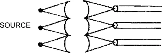
We go through and describe and discuss printer bar where each pixel is imaged onto the detector. See Fig. 1.2.
Figure 1.1 Sources to fiber array.
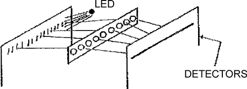
Optical waveguide devices—lens to input and output light from single mode fibers, or arrays thereof. There are a variety of applications, the most important of which is the efficient coupling of light from a laser diode to a single mode fiber. See Fig. 1.3. More recently, these devices are part of the techniques people have used to produce imaging structures, one will see that by virtue of the desired small dimensions, a wide variety of methods become viable which would not be otherwise practical on a larger scale. Examples are binary-optic structures, and to a large extent, gradient index structures. In the case of gradient index, this is easily understood. The focal length of a lens with a parabolically shaped radial profile is proportional to Δn/ΔR, not to Δn itself. Here, Δn/ΔR represents the gradient of the refractive index change with the radius of the lens. Whereas it might be difficult to produce large index differences, it is not required if one can achieve small index differences over small distances. For diffractive lenses which are constructed from periodic structures of the order of wavelengths of light, the resolution capability limits one to 4–5 periods. For a typical case in the visible wavelength range, this limits lens sizes to <100 μm.
Figure 1.3 (a) Fiber array to detector array; (b) Fiber-to-fiber array connector.
In the third part of the book, we single out and discuss two important integrated micro-optic areas. In these chapters, one starts to feel how the new devices utilize and integrate many different types of optical elements as well as share, to a large extent, similarity of fabrication methods. These two chapters will deal with, respectively, the fabrication of microdiffraction gratings, the elements, and properties of optical isolators.
Microgratings and optical isolators have come to the fore, to a large extent, because of the emergence of optical communication systems. As an example, the importance of fiber gratings has come about from the application called “wavelength division multiplexing”, or WDM for short. This has to do with the optical communication scheme where more than one wavelength is propagating in the same optical fiber. The need to separate, and otherwise act independently act on different propagating wavelengths has produced the need for diffraction grating. What is new is that these gratings have to be implemented on a microscale, mated and integrated to an optical system. We will cover all the important methods that have arisen over the last few years to satisfy this new need. Also, we will cover the representative applications.
Chapter 8 will be devoted to an optical device whose need has also arisen from the new “photonic” technology. This technology has to do with the next stage of the optical communication network. This will deal with using light itself to perform many of the functions that are now done electronically. The initial example of this is the optical amplifier. Whatever the particular scheme, it will always need an optical element to prevent light from going backwards in the train that would prematurely de-excite the inverted population. This optical element is the optical isolator. It is included not only to explain another important optical element but also because it provides an excellent example of how many different micro-optic elements are brought together to produce an important new optical device.
The fourth part of the book will be devoted to three new developments in the micro-optic area. The first is that of “photonic crystals” which is covered in the Chapters 9. It is relatively new, even by the standards of the micro-optics field in general, but has made great strides in its short existence. It is an excellent example of the way new innovative technology requires the emergence and push of new methods mixed with new theories, or ways of thinking of old theories. In this case, the new way of thinking about old theories was the realization that the mathematical formulation that is used to determine the behavior of electrons in solids, often called band theory, could also be applied to the way light propagates in periodic structures [5]. The link to the technology of micro-optics is that the length of the periodic scale of the structures for the important case of visible to near infrared wavelengths, corresponds to the wavelength itself. This means that fabrication methods appropriate for many of the elements discussed in the previous chapters are again needed here. To make the cycle complete, the devices that one could imagine using this photonic crystal approach for, are the very same optoelectronic applications discussed in the context of other approaches, which, in turn share the same fabrication techniques. The specific area that has made the greatest progress is that of photonic crystal fibers. From a mere suggestion of the concept four short years ago, there have been demonstrated fibers with losses rivaling the standard optical fiber.
The last two chapters are dedicated to even newer micro-optical phenomena. In Chapters 10, we review the phenomenon of the interaction of short pulse lasers w...