Nano-Semiconductors
eBook - ePub

Nano-Semiconductors

Devices and Technology

  1. 599 pages
  2. English
  3. ePUB (mobile friendly)
  4. Available on iOS & Android
eBook - ePub

Nano-Semiconductors

Devices and Technology

Book details
Book preview
Table of contents
Citations

About This Book

With contributions from top international experts from both industry and academia, Nano-Semiconductors: Devices and Technology is a must-read for anyone with a serious interest in future nanofabrication technologies.

Taking into account the semiconductor industry's transition from standard CMOS silicon to novel device structures—including carbon nanotubes (CNT), graphene, quantum dots, and III-V materials—this book addresses the state of the art in nano devices for electronics. It provides an all-encompassing, one-stop resource on the materials and device structures involved in the evolution from micro- to nanoelectronics.

The book is divided into three parts that address:


  • Semiconductor materials (i.e., carbon nanotubes, memristors, and spin organic devices)
  • Silicon devices and technology (i.e., BiCMOS, SOI, various 3D integration and RAM technologies, and solar cells)
  • Compound semiconductor devices and technology

This reference explores the groundbreaking opportunities in emerging materials that will take system performance beyond the capabilities of traditional CMOS-based microelectronics. Contributors cover topics ranging from electrical propagation on CNT to GaN HEMTs technology and applications. Approaching the trillion-dollar nanotech industry from the perspective of real market needs and the repercussions of technological barriers, this resource provides vital information about elemental device architecture alternatives that will lead to massive strides in future development.

Frequently asked questions

Simply head over to the account section in settings and click on “Cancel Subscription” - it’s as simple as that. After you cancel, your membership will stay active for the remainder of the time you’ve paid for. Learn more here.
At the moment all of our mobile-responsive ePub books are available to download via the app. Most of our PDFs are also available to download and we're working on making the final remaining ones downloadable now. Learn more here.
Both plans give you full access to the library and all of Perlego’s features. The only differences are the price and subscription period: With the annual plan you’ll save around 30% compared to 12 months on the monthly plan.
We are an online textbook subscription service, where you can get access to an entire online library for less than the price of a single book per month. With over 1 million books across 1000+ topics, we’ve got you covered! Learn more here.
Look out for the read-aloud symbol on your next book to see if you can listen to it. The read-aloud tool reads text aloud for you, highlighting the text as it is being read. You can pause it, speed it up and slow it down. Learn more here.
Yes, you can access Nano-Semiconductors by Krzysztof Iniewski in PDF and/or ePUB format, as well as other popular books in Technology & Engineering & Electrical Engineering & Telecommunications. We have over one million books available in our catalogue for you to explore.

Part I

Semiconductor Materials

1 Electrical Propagation on Carbon Nanotubes From Electrodynamics to Circuit Models

Antonio Maffucci, Andrea G. Chiariello, Carlo Forestiere, and Giovanni Miano

CONTENTS

1.1 Introduction
1.2 Electrodynamics of CNTs
1.2.1 Generality
1.2.2 Band Structure of a CNT Shell
1.2.3 Constitutive Relation for a CNT Shell
1.2.4 Number of Effective Channels for SWCNTs and MWCNTs
1.3 An Electromagnetic Application: CNTs as Innovative Scattering Materials
1.3.1 Generality
1.3.2 Electromagnetic Models for CNT Scattering
1.4 Circuital Application: CNTs as Innovative Interconnects
1.4.1 CNTs in Nanointerconnects
1.4.2 TL Model for a CNT Interconnect
1.4.3 A Bundle of CNTs as Innovative Chip-to-Package Interconnects
1.5 Conclusions
References

1.1 INTRODUCTION

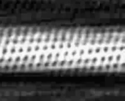
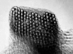
Carbon nanotubes (CNTs) are recently discovered materials [1] made by rolled sheets of graphene of diameters on the order of nanometers and lengths up to millimeters (Figures 1.1 and 1.2). Because of their outstanding electrical, thermal, and mechanical properties [2,3], CNTs have been proposed as emerging materials offering solutions to many of the problems presented by the strict requirements of technology nodes below 22 nm [4,5]. At present, CNTs are considered for a large variety of micro- and nanoelectronics applications, such as nanointerconnects [6–8], nanopackages [9], nanotransistors [10], nanopassives [11], and nanoantennas [12], [13]. Recently, theoretical predictions have been confirmed by the first real-world CNT-based electronic devices, such as the CNT bumps for nanopackaging applications reported by Soga et al. [14] or the CNT wiring of a prototype of digital integrated circuit, one of the first examples of successful CNT-CMOS (complementary metal–oxide–semiconductor) integration [15].
fig1_1
FIGURE 1.1Some real-world nanotubes: AFM image of chiral tube of 1.3 nm diameter (Technical University, Delft). (From Anantram, M.P., and LĂ©onard, F., Rep. Prog. Phys., 69, 507, 2006. With permission.)
Given these perspectives, many attempts have been made to derive models describing the electrical propagation along CNTs. The electromagnetic response of CNTs has been widely examined in frequency ranges from microwave to the visible, properly taking into account the graphene crystalline [16,17]. For each carbon atom in the grapheme, only one out of four valence electrons (the π electron) contributes to the conduction phenomenon; thus, in order to model the electromagnetic response of CNTs, there is the need to describe the interaction of the π electrons with the electromagnetic fields produced by the π electrons themselves and by the external sources, under the action of the electric field generated by the fixed positive ions of the lattice. This requires, in principle, a quantum mechanical approach, since the electrical behavior of π electrons strongly depends on the interaction with the positive ion lattice. A quantum mechanical approach has been used, for instance, in the study of Miyamoto et al. [18], where the model is derived by using numerical simulations based on first principles. Alternatively, phenomenological approaches are possible, such as those proposed by Burke [19,20], based on the Luttinger liquid theory. Another possible option is given by semiclassical approaches, based on simplified models that yield approximated, but analytically tractable, results. Examples are given in Wesström’s report [21], where the CNT is modeled as an electron waveguide, or in Salahuddin et al.’s study [22], where a general model for a quantum wire is derived from the transport theory based on the Boltzmann equation.
fig1_2
FIGURE 1.2Some real-world nanotubes: TEM image of a crystalline nanotube bundle (Rice University). (From Anantram, M.P., and LĂ©onard, F., Rep. Prog. Phys., 69, 507, 2006. With permission.)
Among these models, the fluid ones play a central role in CNT modeling; in fact, despite their simplicity and immediate physical intuition, they are able to describe the main physical processes arising on characteristic lengths involving many unit cells, such as the collective effects. These models assume that the electric fields due to the collective motion of the π electrons themselves and to the external sources are smaller than the atomic crystal field, and also slowly varying on atomic length and time scales. In these conditions, the π electrons behave as “quasi-classical particles” and the equations governing their dynamics are the classical equations of motion, provided that the electron mass is replaced by an “effective mass,” which endows the interaction with the positive ion lattice (e.g., [23]).
Section 1.2 presents an electrodynamical model of the propagation along CNTs, derived by using the above-mentioned semiclassical fluid description. This model was presented by Miano and Villone [23] and Maffucci et al. [24] with reference to small-diameter metallic CNTs, and was heuristically extended by Maffucci et al. [25] to metallic CNTs with large diameters. Following the stream of what was done in several studies [26,27], in this work the model is extended to any type of CNTs, both metallic and semiconducting, with any chirality. The model introduces the concept of “equivalent number of conducting channels,” which represents a measure of the number of subbands in the neighbors of the nanotube Fermi level th...

Table of contents

  1. Cover
  2. Half Title
  3. Title Page
  4. Copyright Page
  5. Table of Contents
  6. Preface
  7. Editor
  8. Contributors
  9. Part I Semiconductor Materials
  10. Part II Silicon Devices and Technology
  11. Part III Compound Semiconductor Devices and Technology
  12. Index