Graphite, the thermodynamically stable phase of carbon at ambient conditions, has been studied and used by humankind for centuries. For instance, during the reign of Queen Elizabeth I, graphite from a large high-quality deposit near Borrowdale in the English Lake District was used as a material to line the moulds for cannonballs. This resulted in rounder and smoother cannonballs than the UK’s military competitors, so production at the mine was strictly controlled by the Crown. To this day, graphite is used for an important and very diverse range of applications such as nuclear reactor moderators, pencils, electric motor brushes and addition of carbon to steel.
1.1.1 Crystal structure of graphite and graphene
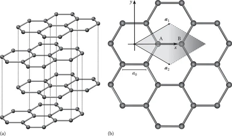
In terms of atomic structure, graphite is a layered material where each layer consists of a hexagonal lattice of carbon atoms joined by strong covalent bonds. The bonds between the layers, on the other hand, are weak van der Waals bonds (Figure 1.1). A single atomic layer of graphite is called graphene. For graphene, we can define a primitive unit cell: the smallest building block from which we can construct the graphene lattice. The primitive unit cell of graphene consists of two atoms due to the hexagonal structure, which we can label as A and B (Figure 1.1). The size of the primitive unit cell of graphite depends on how the individual graphene layers stack to form the graphite crystal. Graphite is found in nature with various stacking arrangements, but in this text we will concentrate on the most common and thermodynamically stable stacking: Bernal (or ABAB) stacking. In Bernal stacking the B atom in the second layer is directly above the A atom in the first layer, and then in the third layer there is an A atom at this location, just as in the first layer. The primitive unit cell of Bernal-stacked graphite thus consists of four atoms in two adjacent layers. The graphite crystal shown in Figure 1.1 exhibits Bernal stacking.
We can define lattice vectors, the vectors joining equivalent points in adjacent unit cells, for mono-layer graphene. Equation 1.1 gives these (two-dimensional) lattice vectors, in terms of the sp2 C–C bond length in graphene a0:
The accepted values [1] for the bond length and lattice constant are a0 = 1.42 Å and a = 2.46 Å. We can also (Equation 1.2) define the reciprocal lattice vectors b1 and b2 for the graphene lattice using the relations a1 ⋅ b1 = 2π, a1 ⋅ b2 = 0, etc. [2]:
Many readers will be familiar with the concept of the reciprocal lattice. The reciprocal lattice of a crystalline material is the Fourier transform of the real space lattice (Appendix C). Whilst the real space lattice is periodic with period determined by the lattice vectors (e.g. those defined in Equation 1.1 for graphene), the reciprocal lattice is periodic with period determined by the reciprocal lattice vectors and has units of wavevector k. Reciprocal space is also referred to as k-space. The physical significance of the reciprocal lattice is that it governs the way in which waves, and particles exhibiting wave–particle duality, propagate through the material. The relationship between energy and wavevector (the dispersion relation) for electrons and phonons propagating in the crystal is periodic with period given by the reciprocal lattice vectors, and the crystal will diffract radiation/particles when the change in wavevector upon diffraction is a reciprocal lattice vector or integer multiples thereof.
It is the role of the reciprocal lattice in determining for what scattering vectors (angles) a crystal will diffract radiation/particles which led to the development of the reciprocal lattice concept. Readers not familiar with the reciprocal lattice concept may wish to read Section 8.1 on the Laue treatment of diffraction, which introduces the concept of the reciprocal lattice by demonstrating its role in understanding diffraction. The reciprocal lattice concept is covered in great detail in the literature [2, 3, 4 and 5].
1.1.2 Electronic properties of graphite and graphene layers
From the electronic point of view, graphite exhibits highly anisotropic behaviour. In the plane of the individual graphene layers, graphite exhibits very high conductivity, whilst in the direction normal to the graphene planes, the conductivity is somewhat lower. The electronic dispersion relation of graphite has been studied theoretically for many decades prior to the isolation of graphene [6, 7 and 8]. As we shall discuss in detail in Chapters 2,3 and 4, graphene features covalent bonding in which three of the four valence electrons form strong directional interatomic bonds (σ-bonds) to neighbouring atoms in the graphene layer. The electrons in the σ-bonds are strongly bound into the bonds so they cannot move. The fourth valence electron, on the other hand, is responsible for weak π-bonds between neighbouring atoms in the graphene layer and weak van der Waals bonds between the graphene layers. The binding energy of these bonds is small so these electrons can easily be excited into the anti-bonding orbital (conduction band) to allow an electric current to flow.
The appropriate methodology to study the electronic dispersion relation of graphite is the tight-binding approximation, which we will use for ourselves in Chapters 3 and 4 and Appendix B. Most ...