- 432 pages
- English
- ePUB (mobile friendly)
- Available on iOS & Android
eBook - ePub
Commercial Wireless Circuits and Components Handbook
About this book
A comprehensive source for microwave and wireless circuit design, the Commercial Wireless Circuits and Components Handbook reviews the fundamentals of transmitters and receivers, then presents detailed chapters on individual circuit types. It also covers packaging, large and small signal characterization, and high volume testing techniques for both devices and circuits. This handbook not only provides important information for engineers working with wireless RF or microwave circuitry, it also serves as an excellent source for those requiring information outside of their area of expertise, such as managers, marketers, and technical support workers who need a better understanding of the fields driving their decisions.
Tools to learn more effectively

Saving Books

Keyword Search

Annotating Text

Listen to it instead
Information
1
Receivers
1.1 Introduction
1.2 Frequency
1.3 Dynamic Range
Power and Gain • Noise • Receiver Noise • Intermodulation • Receiver Intermodulation • Receiver Dynamic Range
1.4 The LO Chain
Amplitude and Phase Noise
1.5 The Potential for Trouble
Electromechanical • Optical Injection • Piezoelectric Effects • Electromagnetic Coupling
1.6 Summary
Motorola GSTG, Inc.
1.1 Introduction
An electromagnetic signal picked up by an antenna is fed into a receiver. The ideal receiver rejects all unwanted noise including other signals. It does not add any noise or interference to the desired signal. The signal is converted, regardless of form or format, to fit the characteristics required by the detection scheme in the signal processor, which in turn feeds an intelligible user interface (Fig. 1.1). The unit must require no new processes, materials, or devices not readily available. This ideal receiver adds no weight, size, or cost to the overall system. In addition, it requires no power source and generates no heat. It has an infinite operating lifetime in any environment, and will never be obsolete. It will be flexible, fitting all past, present, and future requirements. It will not require any maintenance, and will be transparent to the user, who will not need to know anything about it in order to use it. It will be fabricated in an “environmentally friendly” manner, visually pleasing to all who see it, and when the user is finally finished with this ideal receiver, he will be able to recycle it in such a way that the environment is improved rather than harmed. Above all else, this ideal receiver must be wanted by consumers in very large quantities, and it must be extremely profitable to produce. Fortunately, nobody really expects to achieve all of these “ideal” characteristics, at least not yet! However, each of these characteristics must be addressed by the engineering design team in order to produce the best product for the application at hand.
1.2 Frequency
Receivers represent a technology with tremendous variety. They include AM, FM, analog, digital, direct conversion, single and multiple conversions, channelized, frequency agile, spread spectrum, chirp, frequency hopping, and others. The applications are left to the imaginations of the people who create them. Radio, telephones, data links, radar, sonar, TV, astronomical, telemetry, and remote control, are just a few of those applications. Regardless of the application, the selection of the operating frequencies is fundamental to obtaining the desired performance.
The actual receiver frequencies are generally beyond the control of the design team, being dictated, controlled, and even licensed by various domestic or foreign government agencies, or by the customer. When a product is targeted for international markets, the allocated frequencies can take on nightmare qualities due to differing allocations, adjacent interfering bands, and neighboring country restrictions or allocations. It will usually prove impossible to get the ideal frequency for any given application, and often the allocated spectrum will be shared with other users and multiple applications. Often the spectrum is available for a price, usually to the highest bidder. Failure to utilize the purchased spectrum within a specified time frame may result in forfeiture of what is now an asset; an expensive mistake. This has opened up the opportunity to speculate and make (or lose) large sums of money by purchasing spectrum to either control a market or resell to other users. For some applications where frequency allocation is up to the user, atmospheric or media absorption, multipathing, and background noise are important factors that must be considered. These effects can be detrimental or used to advantage. An example includes cross links for use with communications satellites, where the cross link is unaffected by absorption since it is above the atmosphere. However, the frequency can be selected to use atmospheric absorption to provide isolation between ground signals and the satellite cross links. Sorting out these problems is time consuming and expensive, but represents a fundamental first step in receiver design.
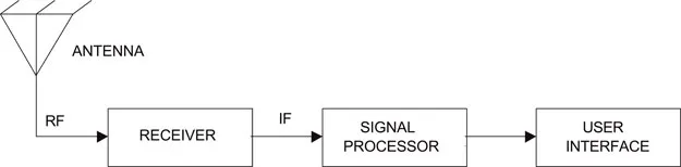
FIGURE 1.1 The receiver.
1.3 Dynamic Range
The receiver should match the dynamic range of the desired signal at the receiver input to the dynamic range of the signal processor. Dynamic range is defined as the range of desirable signal power levels over which the hardware will operate successfully. It is limited by noise, signal compression, and interfering signals and their power levels.
1.3.1 Power and Gain
The power in any signal(s), whether noise, interference or the desired signal, can be measured and expressed in Watts (W), decibels referenced to 1 Watt (dBW), milliwatts (mW) or decibels referenced to one milliwatt (dBm). The power decibel is 10 times the LOG of the dimensionless power ratio. The power gain of a system is the ratio output signal power to the input signal power expressed in decibels (dB). The gain is positive for components in which the output signal is larger than the input, negative if the output signal is smaller. Negative gain is loss, expressed as attenuation (dB). The power gain of a series component chain is found by simple multiplication of the gain ratios, or by summing the decibel gains of the individual components in the chain. All of these relationships are summarized in Fig. 1.2.
1.3.2 Noise
Thermal noise arises from the random movement of charge carriers. The thermal noise power (nT) is usually expressed in dBm (NT), and is the product of Boltzman’s constant (k), system temperature in degrees Kelvin (T), and a system noise bandwidth in Hertz (bn). The system noise bandwidth (bn) is defined slightly different from system bandwidth. It is determined by measuring or calculating the total system thermal average noise power (ntot-ave) over the entire spectrum and dividing it by the system peak average noise power (npk-ave) in a 1 Hz bandwidth. This has the effect of creating a system noise bandwidth in which the noise is all at one level, that of the peak average noise power. For a 1 Hz system noise bandwidth at the input to a system at room temperature (25°C), the thermal noise power is about –174 dBm. These relationships are summarized in Fig. 1.3.
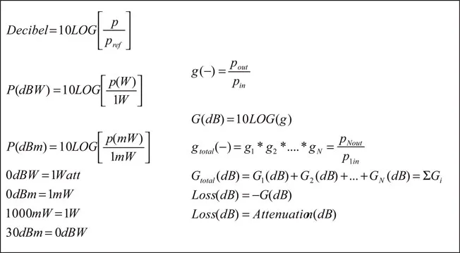
FIGURE 1.2 Power and gain relationships.
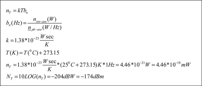
FIGURE 1.3 Noise power relationships.
1.3.3 Receiver Noise
The bottom end of the dynamic range is set by the lowest signal level that can reasonably be expected at the receiver input and by the power level of the smallest acceptably discernible signal as determined at the input to the signal processor. This bottom end is limited by thermal noise at the input, and by the gain distribution and addition of noise as the signal progresses through the receiver. Once a signal is below the minimum discernible signal (MDS) level, it will be lost entirely (except for specialized spread spectrum receivers). The driving requirement is determined by the signal clarity needed at the signal processor. For analog systems, the signal starts to get fuzzy or objectionably noisy at about 10 dB above the noise floor. For digital systems, the allowable bit error rate determines the acceptable margin above the noise floor. Thus the signal with margin sets the threshold minimum desirable signal level.
Noise power at the input to the receiver will be amplified and attenuated like any other signal. Each component in the receiver chain will also add noise. Passive devices such as filters, cables, and attenuators will cause a drop in both signal and noise power alike. These passive devices also contribute a small amount of internally generated thermal noise. Thus the actual noise figure of a passive device is slightly higher than the attenuation of that component. This slight difference is ignored in receiver design since the actual noise figures and losses vary by significantly larger amounts. Passive mixers will generally have a noise figure about 1 dB greater than the conversion loss. Active devices can exhibit loss or gain, and signal and noise power at the input will experience the same effect when transferred to the output. However, the internally generated noise of an active device will be substantial and must be accounted for, requiring reasonably accurate noise figures and gain data on each active component.

FIGURE 1.4 Receiver noise relationships.
The bottom end dynamic range of a receiver component cascade is easily described by the noise equations shown in Fig. 1.4. The first three equations for noise factor (fn), noise figure (NF), and noise temperature (Tn) are equivalent expressions to quantify noise. The noise factor is a dimensionless ratio of the input signal-to-noise ratio and the output signal-to-noise ratio. Replacing the signal ratio with gain results in the final form shown. Noise figure is the decibel form of noise factor, in units of dB. Noise temperature is the conversion of noise factor to an equivalent input temperature that will produce the output noise power, expressed in Kelvin. Convention dictates using noise temperature when discussing antennas and noise figure for receivers and associated electronics. By taking the decibel equivalent of the noise factor, the expression for noise out (No) is obtained, where noise in (Ni) is in dBm and noise figure (NF) and gain (G) are in dB. The cascaded noise factor (ft) is found from the sum of the added noise due to each cascaded component divided by the total gain preceding that element. Use the cascaded noise factor (ft) followed by the noise out (No) equation to determine the noise level at each point in the receiver.
Noise factor is generally computed for a 1 Hz bandwidth and then adjusted for the narrowest filter in the system, which is usually downstream in the signal processor. Occasionally, it will be necessary to account for noise power added to a cascade when components following the narrowest filter have a relatively broad noise bandwidth. The filter will eliminate noise outside its band up to that filter. Broader band components after the filter will add noise back into the system depending on their noise bandwidth. This additional noise can be accounted for using the equation for Δfn-bandwidth, where subscript 1 indicates the narrowband component followed by the wideband component (subscript 2). Repeated application of this equation may be necessary if several wideband components are present following the filter. Image noise can be accounted for using the relationship for Δfn-image where lar is the dimensionless attenuation ratio between the image band and desired signal band and fx is the noise factor of the system up to the image generator (usually a mixer). Not using an image filter in the system will result in a Δfn-image = 2 resulting in a 3 dB increase in noise power. If a filter is used to reject the image by 20 dB, then a substantial reduction in image noise will be achieved. Finally, the corrections for bandwidth and image are easily incorporated using the relationship for the cascaded total noise factor, ftotal.
A simple single sideband (SSB) receiver example, normalized to a 1 Hz noise bandwidth, is shown in Fig. 1.5. It demonstrates the importance of minimizing the use of lossy components near the receiver front end, as well as the importance of a good LNA. A 10 dB output signal-to-noise margin has been established as part of the design. Using the –174 dBm input thermal noise level and the individual component gains and noise figures, the normalized noise level can be traced through the receiver, resulting in an output noise power of –136.9 dBm. Utilizing each component gain and working backwards from this point with a signal results in the MDS power level in the receiver. Adding the 10 dB signal-to-noise margin to the MDS level results in the signal with margin power level as it progresses through the receiver. The signal and noise levels at the receiver input and output are indicated. The design should minimize the gap between the noise floor and the MDS level. Progressing from the input toward the output, it is readily apparent that the noise floor gets closer to and rapidly converges with...
Table of contents
- Cover
- Half Title
- Title Page
- Copyright Page
- Table of Contents
- 1 Re ceivers
- 2 Transmitters
- 3 Low Noise Amplifier Design
- 4 Microwave Mixer Design
- 5 Modulation and Demodulation Circuitry
- 6 Power Amplifier Circuits
- 7 Oscillator Circuits
- 8 Phase Locked Loop Design
- 9 Filters and Multiplexers
- 10 RF Switches
- 11 RF Package Design and Development
- 12 Guided Wave Propagation and Transmission
- 13 Linear Measurements
- 14 Network Analyzer Calibration
- 15 Noise Measurements
- 16 Nonlinear Microwave Measurement and Characterization
- 17 Theory of High-Power Load-Pull Characterization for RF and Microwave Transistors
- 18 Pulsed Measurements
- 19 Microwave On-Wafer Test
- 20 High Volume Microwave Test
- 21 Computer-Aided Design of Passive Components
- 22 Nonlinear RF and Microwave Circuit Analysis
- 23 Computer-Aided Design of Microwave Circuitry
- 24 Nonlinear Transistor Modeling for Circuit Simulation
- Index
Frequently asked questions
Yes, you can cancel anytime from the Subscription tab in your account settings on the Perlego website. Your subscription will stay active until the end of your current billing period. Learn how to cancel your subscription
No, books cannot be downloaded as external files, such as PDFs, for use outside of Perlego. However, you can download books within the Perlego app for offline reading on mobile or tablet. Learn how to download books offline
Perlego offers two plans: Essential and Complete
- Essential is ideal for learners and professionals who enjoy exploring a wide range of subjects. Access the Essential Library with 800,000+ trusted titles and best-sellers across business, personal growth, and the humanities. Includes unlimited reading time and Standard Read Aloud voice.
- Complete: Perfect for advanced learners and researchers needing full, unrestricted access. Unlock 1.4M+ books across hundreds of subjects, including academic and specialized titles. The Complete Plan also includes advanced features like Premium Read Aloud and Research Assistant.
We are an online textbook subscription service, where you can get access to an entire online library for less than the price of a single book per month. With over 1 million books across 990+ topics, we’ve got you covered! Learn about our mission
Look out for the read-aloud symbol on your next book to see if you can listen to it. The read-aloud tool reads text aloud for you, highlighting the text as it is being read. You can pause it, speed it up and slow it down. Learn more about Read Aloud
Yes! You can use the Perlego app on both iOS and Android devices to read anytime, anywhere — even offline. Perfect for commutes or when you’re on the go.
Please note we cannot support devices running on iOS 13 and Android 7 or earlier. Learn more about using the app
Please note we cannot support devices running on iOS 13 and Android 7 or earlier. Learn more about using the app
Yes, you can access Commercial Wireless Circuits and Components Handbook by Mike Golio in PDF and/or ePUB format, as well as other popular books in Technology & Engineering & Electrical Engineering & Telecommunications. We have over one million books available in our catalogue for you to explore.