This book systematically introduces physical characteristics and implementations of III-nitride wide bandgap semiconductor materials and electronic devices, with an emphasis on high-electron-mobility transistors (HEMTs). The properties of nitride semiconductors make the material very suitable for electronic devices used in microwave power amplification, high-voltage switches, and high-speed digital integrated circuits.
eBook - ePub
Nitride Wide Bandgap Semiconductor Material and Electronic Devices
- 392 pages
- English
- ePUB (mobile friendly)
- Available on iOS & Android
eBook - ePub
Nitride Wide Bandgap Semiconductor Material and Electronic Devices
About this book
Trusted by 375,005 students
Access to over 1.5 million titles for a fair monthly price.
Study more efficiently using our study tools.
Information
1
INTRODUCTION
As one of the most important and influential advanced technologies of the twentieth century, the influence and significance of semiconductor technology has extended into the twenty-first century. As the foundation of information society, the semiconductor technology has been pushing the human society forward while changing the production, daily life, interpersonal communication, and even the way of thinking of mankind. Semiconductor materials have been playing a critical role in the development of the semiconductor technology. The first transistor invented in 1947 was based on the semiconductor of germanium (Ge) with a room temperature band gap of 0.66 eV. The first integrated circuit born in 1958 was actually of a mixed type, and the first true monolithic integrated circuit appeared in 1961 and employed germanium. Silicon (Si) with a room temperature band gap of 1.12 eV replaced germanium in 1965 to be the major material for semiconductor integrated circuits, and nowadays, remains the principal semiconductor material in microelectronics. The vast majority of the semiconductor industries, either the integrated circuit or the photovoltaic cell industry, are still based on silicon. Silicon and germanium are generally referred to as the first-generation semiconductors for their comparatively long history of development. The second-generation semiconductors including both gallium arsenide (GaAs, with a room temperature band gap of 1.42 eV) and indium phosphide (InP, with a room temperature band gap of 1.35 eV) were introduced in the 1970s and primarily adopted in ultrahigh-speed devices, microwave power devices, and integrated circuits. InP integrated circuits were not commercially available until 1997. Major progresses in the third-generation (wide band gap) semiconductors such as gallium nitride (GaN, with a room temperature band gap of 3.45 eV) and silicon carbide (SiC, with a room temperature band gap of 3.25 eV for 4H-SiC) have been made since the end of the twentieth century.
Apart from a wider band gap, GaAs has six times higher electron mobility and twice greater saturated drift velocity than silicon (see Table 1.1), and therefore GaAs devices are more suitable for high-frequency operations. GaAs field-effect transistors also have the advantages of low noise, high efficiency, and good linearity. However, GaAs has poor thermal conductivity and breakdown field than the third-generation semiconductors GaN and SiC and is limited in power characteristics. The maximum output power of the GaAs metal–semiconductor field-effect transistor (MESFET) was 1.4 W/mm@8 GHz in the early 1980s (Macksey and Doerbeck 1981). Various attempts to improve performance by various methods only yielded a limited increase in power density with a maximum power density of 1.57 W/[email protected] GHz (Chen et al. 1991) obtained at a compromised operation frequency.
Table 1.1 Physical Parameters for Semiconductors
SEMICONDUCTORS | Si | GaAs | 4H-SiC | GaN |
Band gap Eg (eV) | 1.12 | 1.42 | 3.25 | 3.45 |
Relative dielectric constant ε | 11.4 | 13.1 | 9.7 | 8.9 |
Electron mobility μe [cm2/(V-s)] | 1400 | 8500 | 1020 | 1000(GaN) 2000(AlGaN/GaN) |
Breakdown field EC (MV/cm) | 0.3 | 0.4 | 3.0 | 3.3 |
Thermal conductivity κ [W/(cm⋅K)] | 1.5 | 0.5 | 4.9 | 2.0 |
Electron saturation velocity Vsat (×107cm/s) | 1.0 | 2.0 | 2.0 | 2.0 |
Baliga figure of merit (low-frequency) εμeEc3 | 1 | 16 | 600 | 1450 |
In the early 1990s, a record high power density of 1.8 W/mm@30 GHz was achieved in the InP metal–insulator–semiconductor field-effect transistor (MISFET) with Si3N4 as gate dielectric (Saunier et al. 1990). But InP MISFETs found little practical use due to unstable current–voltage characteristics induced by unavoidable high density interface states. The later developed InP high electron mobility transistor (HEMT) achieved a microwave power density of 1.45 W/mm@30 GHz coupled with excellent current–voltage characteristics (Aina et al. 1992). The superiority in microwave power characteristics of InP to GaAs devices is mainly attributed to the slightly higher breakdown field and electron saturation velocity of InP. However, InP devices are not good enough in microwave high-power applications (Wu 1997). Instead, they are most advantageous at operation frequencies of 100 GHz or even higher, especially in high-speed and low-power mixed analog and digital integrated circuits (Hao et al. 2000).
The focus of research on compound semiconductor electronic devices has been the wide band gap semiconductor devices since the early 1990s. Generally speaking, wide band gap semiconductors refer to the semiconductors with a band gap greater than 2 eV (Baliga 1989). The Baliga figure of merit listed in Table 1.1 is a common parameter for characterizing the capability of the semiconductors in high-frequency high-power applications, and it can be seen that the wide band gap semiconductors GaN and SiC enjoy superb material properties such as a large band gap, a high breakdown voltage, and a high electron saturation velocity and are well suited for microwave/millimeter wave high-power applications.
Research shows that both the cut-off frequency fT and the maximum oscillating frequency fmax of SiC MESFET microwave power devices are within 20 GHz, so SiC MESFETs are suitable for frequencies below 7 GHz. Among Group III nitride semiconductors including GaN, aluminum nitride (AlN), indium nitride (InN), and their alloys, both GaN and AlN are wide band gap semiconductors though InN has a relatively narrow band gap (~0.7 eV). The prevailing GaN electronic devices are HEMTs based on GaN heterostructures (such as AlGaN/GaN or InAlN/GaN) with the two-dimensional electron gas (2DEG) of high mobility and very high carrier sheet density, making GaN HEMTs better suited for high-frequency high-power applications. GaN HEMTs show excellent heat dissipation characteristics when they are grown on high thermal conductivity substrates such as SiC and diamond and also enjoy both high performance and low cost when grown on mature low-cost large-diameter silicon substrates. Therefore, GaN HEMTs are deemed as the most ideal microwave power devices (Figure 1.1).
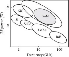
Figure 1.1 Application areas of typical semiconductors. (Reproduced from Nanishi, Y., Present status and challenges of AlGaN/GaN HFETs, Proceedings of the 7th International Conference on Solid-State and Integrated Circuits Technology, Beijing, China, 2004.)
With a band gap range completely covering the entire visible spectrum, Group III nitrides also find wide applications in short wavelength photoelectronic devices that are beyond the capability of conventional semiconductors in addition to high-frequency power applications. In fact, it was the blue light-emitting diode (LED) research that initiated the breakthroughs in Group III nitride semiconductor preparation technologies. Taking the most mature GaN technology for example, the crystalline melting point is over 2500°C (Harafuji et al. 2004), but the decomposition point is in the vicinity of 900°C. Therefore, the conventional melting technique for silicon preparation is not applicable for monocrystal GaN preparation. Of the two GaN preparation methods of bulk crystal growth and heteroepitaxial film growth, the latter saw a breakthrough first with high quality GaN epitaxial films effectively obtained by metalorganic chemical vapor deposition (MOCVD) and molecular beam epitaxy (MBE). The rapid growth of the GaN-based blue LED industry in the 1990s also boosted the GaN electronic device research and development.
Previous researches on Group III nitride electronic devices attempted on various device structures such as MESFET and heterojunction field-effect transistor (HFET), among which the AlGaN/GaN HFET quickly established itself as the mainstream structure for GaN electronic devices. Because of the strong spontaneous polarization and piezoelectric polarization of nitride yields in undoped AlGaN/GaN and InAlN/GaN heterostructures and high-density 2DEGs with significantly higher mobility than that of bulk electrons, the GaN HFETs are more often referred to as GaN HEMTs.
The high conductivity of the 2DEG channel coupled with the high breakdown voltage of GaN makes GaN HEMTs a popular topic in microwave power device researches. The first GaN HEMT was born in 1993 (Khan et al. 1993), and 3 years later, the microwave power characteristics was achieved (Wu et al. 1996). Then, the output power density was improved from the initial 1.1 W/mm@2 GHz to 32.2 W/mm@4 GHz and 30.6 W/mm@8 GHz (Wu et al. 2004), and further to 41.4 W/mm@4 GHz in 2006 (Wu et al. 2006). A total output power of 230 W @2 GHz was achieved in a single GaN HEMT with a gate width of 48 mm (Okamoto et al. 2004).
Such a dramatic progress of nitride electronic devices is attributed first to the continuous improvement of AlGaN/GaN material quality and HEMT technology. Then, the general employment of SiC substrate with better heat dissipation performance contributes significantly to increasing output power. The deposition of dielectric films for surface passivation suppresses the trap-induced current collapse and leads to better microwave performance and reliability. Progress in GaN heterostructures has been made along with the development of heterojunction material epitaxy and device technology. Some techniques such as the insertion of AlN interlayer at AlGaN/GaN heterointerface, the addition of GaN cap layer on surface of AlGaN layer, and the introduction of AlGaN or InGaN back barrier under the GaN channel became popular. Meanwhile, the HEMT structure optimizations such as the gate recess and the field plate also gained wide application. All these improvements pushed the continuous progress of GaN HEMT performance.
The operation frequency, gain, and power including efficiency of GaN HEMTs have also seen gradual increase, with a cut-off frequency of 343 GHz (Shinohara et al. 2011) and a W band output power density of 1.7 W/mm@95 GHz (Brown et al. 2011) reported in 2011. Rapid progress was also witnessed in GaN HEMTs on silicon substrate in an attempt to combine the nitride and silicon technologies. The demand for GaN-based high-speed digital circuits has promoted the development of enhancement-mode GaN HEMTs and enhancement/depletion-mode HEMT circuit units. And the requirement for smaller gate leakage currents has stimulated the research on the GaN metal–oxide–semiconductor HEMT (MOS-HEMT). Better high-frequency characteristics have been achieved in InAlN/GaN HEMT and MIS-HEMTs in recent years by using the nearly lattice-matched InAlN/GaN heterostructure that features a higher 2DEG density and a smaller barrier layer thickness.
Commercial GaN HEMT microwave power devices (on SiC and silicon substrates) were available in 2006 but were far from exerting the potential of GaN HEMTs with the product performance way below the laboratory results of the same period due to many unresolved issues in GaN HEMT performance and reliability. GaN HEMT microwave power device research borrowed much from the material and device physics and fabrication technology of the second-generation semiconductors GaAs, InP, and their heteros...
Table of contents
- Cover
- Half Title
- Title Page
- Copyright Page
- Table of Contents
- PREFACE
- INTRODUCTION
- AUTHORS
- CHAPTER 1 INTRODUCTION
- CHAPTER 2 PROPERTIES OF GROUP III NITRIDE SEMICONDUCTOR MATERIALS
- CHAPTER 3 HETEROEPITAXIAL GROWTH AND DEFECT PROPERTIES OF NITRIDES
- CHAPTER 4 ELECTRICAL PROPERTIES AND RELATED MECHANISMS OF GAN HETEROSTRUCTURES USED IN HIGH ELECTRON MOBILITY TRANSISTORS
- CHAPTER 5 GROWTH AND OPTIMIZATION OF ALGAN/GAN HETEROSTRUCTURES
- CHAPTER 6 ALGAN/GAN MULTIPLE HETEROSTRUCTURE MATERIALS AND ELECTRONIC DEVICES
- CHAPTER 7 GROWTH OF INALN/GAN HETEROSTRUCTURES BY PULSED MOCVD
- CHAPTER 8 DEFECTS AND PHYSICAL PROPERTIES OF GROUP III NITRIDES
- CHAPTER 9 PRINCIPLES AND OPTIMIZATION OF GAN HEMTS
- CHAPTER 10 PREPARATION AND PERFORMANCE OF GAN HEMTS
- CHAPTER 11 ELECTRICAL AND THERMAL DEGRADATION AND RELIABILITY OF GAN HEMTS
- CHAPTER 12 ENHANCEMENT-MODE GAN HEMTS AND INTEGRATED CIRCUITS
- CHAPTER 13 GAN METAL–OXIDE–SEMICONDUCTOR HIGH ELECTRON MOBILITY TRANSISTORS
- CHAPTER 14 DEVELOPMENT OF NITRIDE SEMICONDUCTOR MATERIALS AND ELECTRONIC DEVICES
- INDEX
Frequently asked questions
Yes, you can cancel anytime from the Subscription tab in your account settings on the Perlego website. Your subscription will stay active until the end of your current billing period. Learn how to cancel your subscription
No, books cannot be downloaded as external files, such as PDFs, for use outside of Perlego. However, you can download books within the Perlego app for offline reading on mobile or tablet. Learn how to download books offline
Perlego offers two plans: Essential and Complete
- Essential is ideal for learners and professionals who enjoy exploring a wide range of subjects. Access the Essential Library with 800,000+ trusted titles and best-sellers across business, personal growth, and the humanities. Includes unlimited reading time and Standard Read Aloud voice.
- Complete: Perfect for advanced learners and researchers needing full, unrestricted access. Unlock 1.5M+ books across hundreds of subjects, including academic and specialized titles. The Complete Plan also includes advanced features like Premium Read Aloud and Research Assistant.
We are an online textbook subscription service, where you can get access to an entire online library for less than the price of a single book per month. With over 1.5 million books across 990+ topics, we’ve got you covered! Learn about our mission
Look out for the read-aloud symbol on your next book to see if you can listen to it. The read-aloud tool reads text aloud for you, highlighting the text as it is being read. You can pause it, speed it up and slow it down. Learn more about Read Aloud
Yes! You can use the Perlego app on both iOS and Android devices to read anytime, anywhere — even offline. Perfect for commutes or when you’re on the go.
Please note we cannot support devices running on iOS 13 and Android 7 or earlier. Learn more about using the app
Please note we cannot support devices running on iOS 13 and Android 7 or earlier. Learn more about using the app
Yes, you can access Nitride Wide Bandgap Semiconductor Material and Electronic Devices by Yue Hao,Jin Feng Zhang,Jin Cheng Zhang in PDF and/or ePUB format, as well as other popular books in Technologie et ingénierie & Technologies de l'information. We have over 1.5 million books available in our catalogue for you to explore.