- 242 pages
- English
- ePUB (mobile friendly)
- Available on iOS & Android
eBook - ePub
Simplified Design of Data Converters
About this book
Simplified Design of Data Converters shows how to design and experiment with data converters, both analog-to-digital and digital to analog. The design approach here is the same one used in all of John Lenk's best-selling books on simplified and practical design. Throughout the book, design problems start with guidelines for selecting all components on a trial-value basis, assuming a specific design goal and set of conditions. Then, using the guideline values in experimental circuits, the desired results are produced by varying the experimental component values, if needed.
If you are a working engineer responsible for designing data-converters circuits, or selecting IC data converters, the variety of circuit configurations described here should generally simplify your task. Not only does the book describe converter-circuit designs, but it also covers the most popular forms of data-converter ICs available. Throughout the book, you will find a wealth of information on data-converter ICs and related components.
- For all skill levels
- Tells how to design and build data-converter circuits from scratch
Tools to learn more effectively

Saving Books

Keyword Search

Annotating Text

Listen to it instead
Information
CHAPTER 1
Data Converter Basics
This chapter is devoted to basic data converters, both analog-to-digital and digital-to-analog. The chapter is primarily for readers who are totally unfamiliar with data converters. It is possible to design data-converter circuits from scratch. However, data converters are available in integrated circuit (IC) form, and it is generally simpler to use such ICs.
The data sheets for IC converters often show the connections and provide all necessary design parameters to produce complete converter circuits by adding external components. This chapter describes the function and operation of IC converters to help you understand the data sheet information.
Before we get started, let us resolve certain differences in terms. Some manufacturers refer to analog-to-digital converters as ADCs. Other manufactures use the term A/D converter. The same is true of digital-to-analog converters, which are referred to as DACs by some, and as D/A converters by others. I prefer the terms ADC and DAC, but do not be surprised to find both terms in this book.
1.1 Basic Data Conversion Techniques
This section describes the various ADC and DAC techniques in common use. Here we concentrate on explanations of the basic principles of data conversion. By studying this information, you should be able to understand operation of the converter IC described throughout the book. It is assumed that you are familiar with basic digital electronics. If not, read Lenk’s Digital Handbook (McGraw-Hill, 1993).
1.1.1 Typical BCD Signal Formats Used in ADC/DAC Circuits
Figure 1-1a shows the relationship of the three most common BCD (binary coded decimal) signal formats: NRZL (nonreturn-to-zero level), NRZM (nonreturn-to-zero-mark), and RZ (return-to-zero).
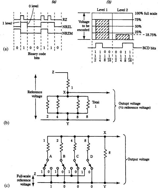
FIGURE 1-1 ADC and DAC conversion basics
In NRZL, a 1 is one signal level, and a 0 is another signal level. These levels can be 5 V, 10 V, 0 V, −5 V, or any other selected values, provided that the 1 and 0 levels are entirely different.
In RZ, a 1-bit is represented by a pulse of definite width (usually a ½-bit width) that returns to zero signal level, and the 0-bit is represented by a zero-level signal.
In NRZM, the level of the pulse has no meaning. A 1 is represented by a change in level, and a 0 is represented by no change.
1.1.2 Four-Bit System in the Conversion Process
Figure 1-1b shows the relation between two voltage levels to be converted, and the corresponding binary code (in NRZL form), in a basic ADC. In practice, a four-bit ADC (sometimes called a binary encoder) samples the voltage level to be converted and compares the voltage to ½ scale, ¼ scale, 1/8 scale, and 1/16 scale (in that order) of a given full-scale voltage. The ADC then produces four data bits, in sequence, with the comparison made on the most significant (½ scale) first.
As shown in Fig. 1-1b, each of the two voltage levels is divided into four equal time increments. The first time increment is used to represent the ½-scale bit, the second increments the ¼-scale, and so on.
In voltage level 1, the first two time increments are at binary 1, and the second two increments are at 0. This produces 1100, or decimal 12. Twelve is ¾ of 16. Thus level 1 is 75% of full scale. For example, if full scale is 10 V, level 1 is 7.5 V.
In level 2, the first two increments are at 0, and the second two increments are at 1. This is represented as 0011, or 3. Thus level 2 is 1/16 of full scale (or 1.875 V). This can be expressed in another way. In the first or ½-scale increment, the converter produces a 0 because the voltage (1.875 V) is less than ½ scale (5 V). The same is true of the second or ¼-scale increment (1.875 V is less than 2.5 V).
In the third or 1/8-scale increment of level 2, the converter produces a 1, as it does in the fourth or 1/8-scale increment, because the voltage being compared is greater than 1/8 of full scale (1.875 is greater than 0.625 V). Thus the ½- and ¼-scale increments are at 0, and the 1/8- and 1/16-scale increments are at 1 (also, 1/8 + 1/16 = 3/16 or 18.75%).
1.1.3 ADC Conversion Ladder
Figure 1-1c shows a conversion ladder, which is the heart of many ADC circuits. The ladder provides a means of implementing a four-bit binary-coding system and produces an output that is equivalent to switch positions. The switches can be moved to either a 1 or a 0 position, which corresponds to a four-place binary number. The output voltage describes a percentage of the full-scale reference voltage, depending on the switch positions. For example, if all switches are at 0 position, there is no output voltage. This produces a binary 0000, represented by 0 V.
If switch A is at 1 and the remaining switches are at 0, this produces a binary 1000 (decimal 8). Because the total in a four-bit system is 16 (0 to 15), 8 represents ½ full scale. Thus the output voltage is ½ the full-scale reference voltage. This conversion is done as follows.
The 2-, 4-, and 8-ohm switch resistors and the 8-ohm output resistor are connected in parallel. This produces a value of 1 ohm across points X and Y. The reference voltage is applied across the 1-ohm switch resistor (across points Z and X) and the 1-ohm combination of resistors (acro...
Table of contents
- Cover image
- Title page
- Table of Contents
- The EDN Series for Design Engineers
- Copyright
- Dedication
- Preface
- Acknowledgments
- Chapter 1: Data Converter Basics
- Chapter 2: Data-Converter Terms and Design Characteristics
- Chapter 3: Practical Design Considerations
- Chapter 4: Simplified Design with a Typical ADC
- Chapter 5: Simplified Design with a Flash ADC
- Chapter 6: Simplified Design with Serial-Interface DAC
- Chapter 7: Simplified Design with Parallel-Input DAC
- Chapter 8: Simplified Design Approaches
- Chapter 9: Low-Power Data-Acquisition System
- Chapter 10: Single-Chip Digital Multimeter
- For Further Information
- Index
Frequently asked questions
Yes, you can cancel anytime from the Subscription tab in your account settings on the Perlego website. Your subscription will stay active until the end of your current billing period. Learn how to cancel your subscription
No, books cannot be downloaded as external files, such as PDFs, for use outside of Perlego. However, you can download books within the Perlego app for offline reading on mobile or tablet. Learn how to download books offline
Perlego offers two plans: Essential and Complete
- Essential is ideal for learners and professionals who enjoy exploring a wide range of subjects. Access the Essential Library with 800,000+ trusted titles and best-sellers across business, personal growth, and the humanities. Includes unlimited reading time and Standard Read Aloud voice.
- Complete: Perfect for advanced learners and researchers needing full, unrestricted access. Unlock 1.4M+ books across hundreds of subjects, including academic and specialized titles. The Complete Plan also includes advanced features like Premium Read Aloud and Research Assistant.
We are an online textbook subscription service, where you can get access to an entire online library for less than the price of a single book per month. With over 1 million books across 990+ topics, we’ve got you covered! Learn about our mission
Look out for the read-aloud symbol on your next book to see if you can listen to it. The read-aloud tool reads text aloud for you, highlighting the text as it is being read. You can pause it, speed it up and slow it down. Learn more about Read Aloud
Yes! You can use the Perlego app on both iOS and Android devices to read anytime, anywhere — even offline. Perfect for commutes or when you’re on the go.
Please note we cannot support devices running on iOS 13 and Android 7 or earlier. Learn more about using the app
Please note we cannot support devices running on iOS 13 and Android 7 or earlier. Learn more about using the app
Yes, you can access Simplified Design of Data Converters by John Lenk in PDF and/or ePUB format, as well as other popular books in Diseño & Tratamiento de datos. We have over one million books available in our catalogue for you to explore.