Introduction
So why in a book about CUDA are we looking at supercomputers? Supercomputers are typically at the leading edge of the technology curve. What we see here is what will be commonplace on the desktop in 5 to 10 years. In 2010, the annual International Supercomputer Conference in Hamburg, Germany, announced that a NVIDIA GPU-based machine had been listed as the second most powerful computer in the world, according to the top 500 list (http://www.top500.org). Theoretically, it had more peak performance than the mighty IBM Roadrunner, or the then-leader, the Cray Jaguar, peaking at near to 3 petaflops of performance. In 2011, NVIDIA CUDA-powered GPUs went on to claim the title of the fastest supercomputer in the world. It was suddenly clear to everyone that GPUs had arrived in a very big way on the high-performance computing landscape, as well as the humble desktop PC.
Supercomputing is the driver of many of the technologies we see in modern-day processors. Thanks to the need for ever-faster processors to process ever-larger datasets, the industry produces ever-faster computers. It is through some of these evolutions that GPU CUDA technology has come about today.
Both supercomputers and desktop computing are moving toward a heterogeneous computing route—that is, they are trying to achieve performance with a mix of CPU (Central Processor Unit) and GPU (Graphics Processor Unit) technology. Two of the largest worldwide projects using GPUs are BOINC and Folding@Home, both of which are distributed computing projects. They allow ordinary people to make a real contribution to specific scientific projects. Contributions from CPU/GPU hosts on projects supporting GPU accelerators hugely outweigh contributions from CPU-only hosts. As of November 2011, there were some 5.5 million hosts contributing a total of around 5.3 petaflops, around half that of the world’s fastest supercomputer, in 2011, the Fujitsu “K computer” in Japan.
The replacement for Jaguar, currently the fastest U.S. supercomputer, code-named Titan, is planned for 2013. It will use almost 300,000 CPU cores and up to 18,000 GPU boards to achieve between 10 and 20 petaflops per second of performance. With support like this from around the world, GPU programming is set to jump into the mainstream, both in the HPC industry and also on the desktop.
You can now put together or purchase a desktop supercomputer with several teraflops of performance. At the beginning of 2000, some 12 years ago, this would have given you first place in the top 500 list, beating IBM ASCI Red with its 9632 Pentium processors. This just shows how much a little over a decade of computing progress has achieved and opens up the question about where we will be a decade from now. You can be fairly certain GPUs will be at the forefront of this trend for some time to come. Thus, learning how to program GPUs effectively is a key skill any good developer needs to acquire.
Von Neumann Architecture
Almost all processors work on the basis of the process developed by Von Neumann, considered one of the fathers of computing. In this approach, the processor fetches instructions from memory, decodes, and then executes that instruction.
A modern processor typically runs at anything up to 4 GHz in speed. Modern DDR-3 memory, when paired with say a standard Intel I7 device, can run at anything up to 2 GHz. However, the I7 has at least four processors or cores in one device, or double that if you count its hyperthreading ability as a real processor.
A DDR-3 triple-channel memory setup on a I7 Nehalem system would produce the theoretical bandwidth figures shown in Table 1.1. Depending on the motherboard, and exact memory pattern, the actual bandwidth could be considerably less.
Table 1.1 Bandwidth on I7 Nehalem Processor
| QPI Clock | Theoretical Bandwidth | Per Core |
4.8 GT/s
(standard part) | 19.2 GB/s | 4.8 GB/s |
6.4 GT/s
(extreme edition) | 25.6 GB/s | 6.4 GB/s |
Note: QPI = Quick Path Interconnect.
You run into the first problem with memory bandwidth when you consider the processor clock speed. If you take a processor running at 4 GHz, you need to potentially fetch, every cycle, an instruction (an operator) plus some data (an operand).
Each instruction is typically 32 bits, so if you execute nothing but a set of linear instructions, with no data, on every core, you get 4.8 GB/s ÷ 4 = 1.2 GB instructions per second. This assumes the processor can dispatch one instruction per clock on average∗. However, you typically also need to fetch and write back data, which if we say is on a 1:1 ratio with instructions, means we effectively halve our throughput.
The ratio of clock speed to memory is an important limiter for both CPU and GPU throughput and something we’ll look at later. We find when you look into it, most applications, with a few exceptions on both CPU and GPU, are often memory bound and not processor cycle or processor clock/load bound.
CPU vendors try to solve this problem by using cache memory and burst memory access. This exploits the principle of locality. It you look at a typical C program, you might see the following type of operation in a function:
void some_function
{
int array[100];
int i = 0;
for (i=0; i<100; i++)
{
array[i] = i ∗ 10;
}
}
If you look at how the processor would typically implement this, you would see the address of array loaded into some memory access register. The parameter i would be loaded into another register. The loop exit condition, 100, is loaded into another register or possibly encoded into the instruction stream as a literal value. The computer would then iterate around the same instructions, over and over again 100 times. For each value calculated, we have control, memory, and calculation instructions, fetched and executed.
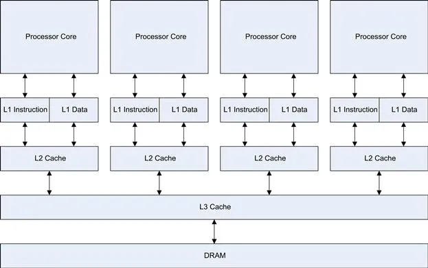
This is clearly inefficient, as the computer is executing the same instructions, but with different data values. Thus, the hardware designers implement into just about all processors a small amount of cache, and in more complex processors, many levels of cache (Figure 1.1). When the processor would fetch something from memory, the processor first queries the cache, and if the data or instructions are present there, the high-speed cache provides them to the processor.
Figure 1.1 Typical modern CPU cache organization.
If the data is not in the first level (L1) cache, then a fetch from the second or third level (L2 or L3) cache is required, or from the main memory if no cache line has this data already. The first level cache typically runs at or near the processor clock speed, so for the execution of our loop, potentially we do get near the full processor speed, assuming we write cache as well as read cache. However, there is a cost for this: The size of the L1 cache is typically only 16 K or 32 K in size. The L2 cache is somewhat slower, but much larger, typically around 256 K. The L3 cache is much larger, usually several megabytes in size, but again much slower than the L2 cache.
With real-life examples, the loop iterations are much, much larger, maybe many megabytes in size. Even if the program can remain in cache memory, the dataset usually cannot, so the processor, despite all this cache trickery, is quite often limited by the memory throughput or bandwidth.
When the processor fetches an instruction or data item from the cache instead of the main memory, it’s called a cache hit. The incremental benefit of using progressively larger caches drops off quite rapidly. This in turn means the ever-larger caches we see on modern processors are a less and less useful means to improve performance, unless they manage to encompass the entire dataset of the problem.
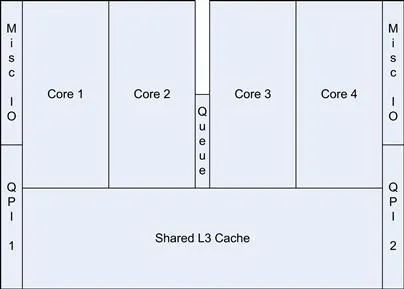
The Intel I7-920 processor has some 8 MB of internal L3 cache. This cache memory is not free, and if we look at the die for the Intel I7 processor, we see around 30% of the size of the chip is dedicated to the L3 cache memory (Figure 1.2).
Figure 1.2 Layout of I7 Nehalem processor on processor die.
As cache sizes grow, so does the physical size of the silicon used to make the processors. The larger the chip, the more expensive it is to manufacture and the higher the likelihood that it will contain an error and be discarded during the manufacturing process. Sometimes these faulty devices are sold cheaply as either triple- or dual-core devices, with the faulty cores disabled. However, the effect of larger, progressively more inefficient caches ultimately results in higher costs to the end user.
Cray
The computing revolution that we all know today started back in the 1950s with the advent of the first microprocessors. These devices, by today’s standards, are slow and you most likely have a far more powerful processor in your smartphone. However, these led to the evolution of supercomputers, which are machines usually owned by governments, large academic institutions, or corporations. They are thousands of times more powerful than the computers in general use today. They cost millions of dollars to produce, occupy huge amounts of space, usually have special cooling requirements, and require a team of engineers to look after them. They consume huge amounts of power, to the extent they are often as expensive to run each year as they cost to build. In fact, power is one of the key considerations when planning such an installation and one of the main limiting factors in the growth of today’s supercomputers.
One of the founders of modern supercomputers was Seymour Cray with his Cray-1, produced by Cray Research back in 1976. It had many thousands of individual cables required to connect everything together—so much so they used to employ women because their hands were smaller than those of most men and they could therefore more easily wire up all the thousands of individual cables.
These machines would typically have an uptime (the actual running time between breakdowns) measured in hours. Keeping them running for a whole day at a time would be considered a huge
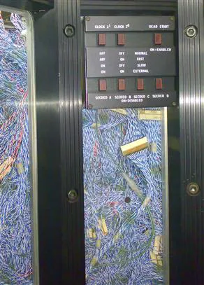
Figure 1.3 Wiring inside the Cray-2 supercomputer.
achievement. This seems quite backward by today’s standards. However, we owe a lot of what we have today to research carried out by Seymour Cray and other individuals of this era.
Cray went on to produce some of the most groundbreaking supercomputers of his time under various Cray names. The original Cray-1 cost some $8.8 million USD and achieved a massive 160 MFLOPS (million floating-point operations per second). Computing speed today is measured in TFLOPS (tera floating-point operations per second), a million times larger than the old MFLOPS measurement (1012 vs. 106). A single Fermi GPU card today has a theoretical peak in excess of 1 teraflop of performance.
The Cray-2 was a significant improvement on the Cray-1. It used a shared memory architecture, split into banks. These were connected to one, two, or four processors. It led the way for the creation of today’s server-based symmetrical multiprocessor (SMP) systems in which multiple CPUs shared the same memory space. Like many machines of its era, it was a vector-based machine. In a vector machine the same operation acts on many operands. These still exist today, in part as processor extensions such as MMX, SSE, and AVX. GPU devices are, at their heart, vector processors that share many similarities with the older supercomputer designs.
The Cray also had hardware support for sc...