eBook - ePub
Linear Circuit Design Handbook
- 960 pages
- English
- ePUB (mobile friendly)
- Available on iOS & Android
eBook - ePub
Linear Circuit Design Handbook
About this book
This book enables design engineers to be more effective in designing discrete and integrated circuits by helping them understand the role of analog devices in their circuit design. Analog elements are at the heart of many important functions in both discrete and integrated circuits, but from a design perspective the analog components are often the most difficult to understand. Examples include operational amplifiers, D/A and A/D converters and active filters. Effective circuit design requires a strong understanding of the operation of these analog devices and how they affect circuit design.
- Comprehensive coverage of analog circuit components for the practicing engineerMarket-validated design information for all major types of linear circuitsIncludes practical advice on how to read op amp data sheets and how to choose off-the-shelf op ampsFull chapter covering printed circuit board design issues
Tools to learn more effectively

Saving Books

Keyword Search

Annotating Text

Listen to it instead
Information
CHAPTER 1 The Op Amp

Chapter Introduction
In this chapter we will discuss the basic operation of the op amp, one of the most common linear design building blocks.
In Section 1-1 the basic operation of the op amp will be discussed. We will concentrate on the op amp from the black box point of view. There are a good many texts that describe the internal workings of an op amp, so in this work a more macro view will be taken. There are a couple of times, however, that we will talk about the insides of the op amp. It is unavoidable.
In Section 1-2 the basic specifications will be discussed. Some techniques to compensate for some of the op amps limitations will also be given.
Section 1-3 will discuss how to read a data sheet. The various sections of the data sheet and how to interpret what is written will be discussed.
Section 1-4 will discuss how to select an op amp for a given application.
SECTION 1-1 Op Amp Operation
Introduction
The op amp is one of the basic building blocks of linear design. In its classic form it consists of two input terminals—one of which inverts the phase of the signal, the other preserves the phase—and an output terminal. The standard symbol for the op amp is given in Figure 1-1. This ignores the power supply terminals, which are obviously required for operation.
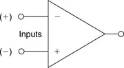
Figure 1-1: Standard op amp symbol
The name “op amp” is the standard abbreviation for operational amplifier. This name comes from the early days of amplifier design, when the op amp was used in analog computers. (Yes, the first computers were analog in nature, rather than digital.) When the basic amplifier was used with a few external components, various mathematical “operations” could be performed. One of the primary uses of analog computers was during World War II, when they were used for plotting ordinance trajectories.
Voltage Feedback Model
The classic model of the voltage feedback (VFB) op amp incorporates the following characteristics:
1. Infinite input impedance
2. Infinite bandwidth
3. Infinite gain
4. Zero output impedance
5. Zero power consumption
None of these can be actually realized, of course. How close we come to these ideals determines the quality of the op amp.
This is referred to as the VFB model. This type of op amp comprises nearly all op amps below 10 MHz bandwidth and on the order of 90% of those with higher bandwidths (Figure 1-2).
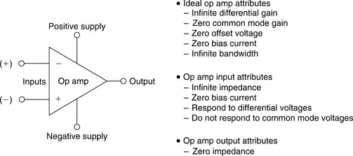
Figure 1-2: The attributes of an ideal op amp
Basic Operation
The basic operation of the op amp can be easily summarized. First we assume that there is a portion of the output that is feedback to the inverting terminal to establish the fixed gain for the amplifier. This is negative feedback. Any differential voltage across the input terminals of the op amp is multiplied by the amplifier’s open-loop gain. If the magnitude of this differential voltage is more positive on the inverting (−) terminal than on the non-inverting (+) terminal, the output will go more negative. If the magnitude of the differential voltage is more positive on the non-inverting (+) terminal than on the inverting (−) terminal, the output voltage will become more positive. The open-loop gain of the amplifier will attempt to force the differential voltage to zero. As long as the inouts and output stays in the operational range of the amplifier, it will keep the differential voltage at zero and the output will be the input voltage multiplied by the gain set by the feedback. Note from this that the inputs respond to differential-mode not common-mode input voltage:

Inverting and Non-Inverting Configurations
There are two basic ways configure the VFB op amp as an amplifier. These are shown in Figure 1-3 and Figure 1-4.
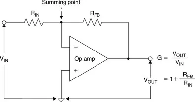
Figure 1-3: Inverting-mode op amp stage
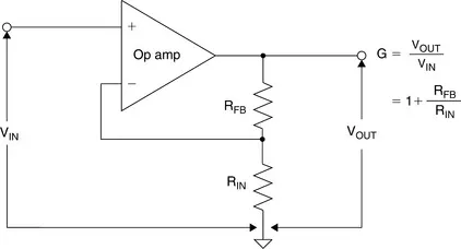
Figure 1-4: Non-inverting-mode op amp stage
Figure 1-3 shows what is known as the inverting configuration. With this circuit, the output is out of phase with the input. The gain of this circuit is determined by the ratio of the resistors used and is given by:

Figure 1-4 shows what is know as the non-inverting configuration. With this circuit, the output is in phase with the input. The gain of the circuit is also determined by the ratio of the resistors used and is given by:

Note that since the output drives a voltage divider (the gain setting network) the maximum voltage available at the inverting terminal is the full output voltage, which yields a minimum gain of 1.
Also note that in both cases the feedback is from the output to the inverting terminal. This is negative feedback and has many advantages for the designer. These will be discussed in more detail further in this chapter.
It should also be noted that the gain is based on the ratio of the resistors, not their actual values. This means that the designer can choose just about any value he or she wishes within practical limits.
If the value of the resistors is too low, a great deal of current would be required from the op amps outpu...
Table of contents
- Cover image
- Title page
- Table of Contents
- Copyright
- Preface
- Chapter 1: The Op Amp
- Chapter 2: Other Linear Circuits
- Chapter 3: Sensors
- Chapter 4: RF/IF Circuits
- Chapter 5: Fundamentals of Sampled Data Systems
- Chapter 6: Converters
- Chapter 7: Data Converter Support Circuits
- Chapter 8: Analog Filters
- Chapter 9: Power Management
- Chapter 10: Passive Components
- Chapter 11: Overvoltage Effects on Analog Integrated Circuits
- Chapter 12: Printed Circuit-Board Design Issues
- INDEX
Frequently asked questions
Yes, you can cancel anytime from the Subscription tab in your account settings on the Perlego website. Your subscription will stay active until the end of your current billing period. Learn how to cancel your subscription
No, books cannot be downloaded as external files, such as PDFs, for use outside of Perlego. However, you can download books within the Perlego app for offline reading on mobile or tablet. Learn how to download books offline
Perlego offers two plans: Essential and Complete
- Essential is ideal for learners and professionals who enjoy exploring a wide range of subjects. Access the Essential Library with 800,000+ trusted titles and best-sellers across business, personal growth, and the humanities. Includes unlimited reading time and Standard Read Aloud voice.
- Complete: Perfect for advanced learners and researchers needing full, unrestricted access. Unlock 1.4M+ books across hundreds of subjects, including academic and specialized titles. The Complete Plan also includes advanced features like Premium Read Aloud and Research Assistant.
We are an online textbook subscription service, where you can get access to an entire online library for less than the price of a single book per month. With over 1 million books across 990+ topics, we’ve got you covered! Learn about our mission
Look out for the read-aloud symbol on your next book to see if you can listen to it. The read-aloud tool reads text aloud for you, highlighting the text as it is being read. You can pause it, speed it up and slow it down. Learn more about Read Aloud
Yes! You can use the Perlego app on both iOS and Android devices to read anytime, anywhere — even offline. Perfect for commutes or when you’re on the go.
Please note we cannot support devices running on iOS 13 and Android 7 or earlier. Learn more about using the app
Please note we cannot support devices running on iOS 13 and Android 7 or earlier. Learn more about using the app
Yes, you can access Linear Circuit Design Handbook by Analog Devices Inc. Analog Devices Inc. Engineeri,Analog Devices Inc., Engineeri, Hank Zumbahlen in PDF and/or ePUB format, as well as other popular books in Technology & Engineering & Industrial Design. We have over one million books available in our catalogue for you to explore.