eBook - ePub
Wide Bandgap Semiconductor Power Devices
Materials, Physics, Design, and Applications
- 418 pages
- English
- ePUB (mobile friendly)
- Available on iOS & Android
eBook - ePub
Wide Bandgap Semiconductor Power Devices
Materials, Physics, Design, and Applications
About this book
Wide Bandgap Semiconductor Power Devices: Materials, Physics, Design and Applications provides readers with a single resource on why these devices are superior to existing silicon devices. The book lays the groundwork for an understanding of an array of applications and anticipated benefits in energy savings. Authored by the Founder of the Power Semiconductor Research Center at North Carolina State University (and creator of the IGBT device), Dr. B. Jayant Baliga is one of the highest regarded experts in the field. He thus leads this team who comprehensively review the materials, device physics, design considerations and relevant applications discussed.
- Comprehensively covers power electronic devices, including materials (both gallium nitride and silicon carbide), physics, design considerations, and the most promising applications
- Addresses the key challenges towards the realization of wide bandgap power electronic devices, including materials defects, performance and reliability
- Provides the benefits of wide bandgap semiconductors, including opportunities for cost reduction and social impact
Trusted by 375,005 students
Access to over 1.5 million titles for a fair monthly price.
Study more efficiently using our study tools.
Information
1
Introduction
B. Jayant Baliga, North Carolina State University, Raleigh, NC, United States
Abstract
The application spectrum for wide bandgap semiconductor power devices is described in terms of operating frequency and power-handling capability. The basic structures for wide bandgap semiconductor power diodes and switches are described. The commercially available silicon carbide devices have a vertical architecture while the gallium nitride devices have a lateral structure. The commercially available silicon carbide devices diodes use the junction barrier controlled Schottky concept. The commercially available silicon carbide power metal oxide semiconductor field effect transistors (MOSFETs) utilize a P+ shielding region to prevent P-base reach-through and high electric field in the gate oxide. The lateral GaN devices are high electron mobility transistors (HEMT) structures that achieve large mobility and sheet charge in the channel and drift region. Depletion-mode GaN HEMT devices are paired with silicon power MOSFETs in the Baliga-Pair (or cascode) configuration to achieve a normally-off switch for applications.
Keywords
Power devices; silicon carbide; gallium nitride; JBS diodes; power MOSFETs; HEMT; Baliga-Pair; cascade
1.1 Silicon power devices
Efficient electrical power generation, distribution, and management has become essential in modern society. These functions were first served by the development of bipolar silicon power devices to displace vacuum tubes in the 1950s. The ratings of silicon bipolar transistors and thyristors grew rapidly to serve an ever broader system need. However, their fundamental limitations in terms of the cumbersome control and protection circuitry led to bulky and costly solutions. A new class of devices evolved in the 1970s for power switching applications with the advent of metal oxide semiconductor (MOS) technology for digital circuits. These silicon power metal oxide semiconductor field effect transistors (MOSFETs) have found extensive use in high frequency applications with relatively low operating voltages (under 100 V). The merger of MOS and bipolar physics enabled creation of yet another class of silicon devices in the 1980s. The most successful innovation in this class of devices has been the insulated gate bipolar transistor (IGBT) [1]. The high power density, simple interface, and ruggedness of the IGBT have made it the technology of choice for all medium and high power applications.
In the 1990s, the concept of two-dimensional charge coupling was introduced using two basic approaches to significantly reduce the on-state resistance of silicon power devices. The first approach utilized a source connected electrode embedded inside a deep vertical trench. This method enabled a new generation of silicon power devices that have been commercialized with voltage ratings of 30–200 V. The second approach utilized alternating vertical columns of P- and N-type silicon regions. Products with blocking voltage around 600 V have been commercialized using this method. Any wide bandgap semiconductor power devices must outperform these advanced silicon power devices now available in the market.
1.2 Silicon power device applications
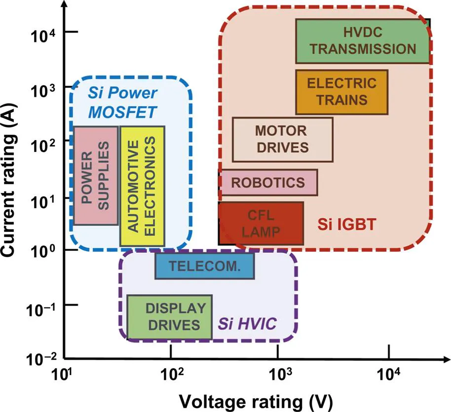
Power devices are used in all sectors of the economy with systems that operate over a broad spectrum of power levels and frequencies. The applications for power devices are shown as a function of operating frequency in Fig. 1.1. High voltage direct current (HVDC) power distribution and locomotive drives that require the control of megawatts of power operate at relatively low frequencies. The power ratings decrease for the devices when the operating frequency increases with typical microwave devices handling about 100 W. All of these applications are served by silicon devices today. Power MOSFETs are preferred for the high frequency applications operating from low power source voltages. These applications include power supplies for computers and laptops, power management in smart phones, and automotive electronics. Until recently, thyristors were the only devices available with sufficient voltage and current ratings favored for the HVDC power distribution applications. The ratings of IGBTs have now grown to levels where they are now preferred over thyristors for voltage source converters and flexible alternating current transmission (FACTs) designs. The medium frequency and power applications such as electric trains, hybrid-electric cars, home appliances, compact fluorescent lamps, medical equipment, and industrial motor drives also utilize the IGBT.

Silicon power devices can also be classified based on their current and voltage-handling requirements as shown in Fig. 1.2. Thyristors are available that can individually handle over 6000 V and 2000 A enabling the control of over 10 MW of power by a single monolithic device. These devices are suitable for the HVDC power transmission applications. During last 10 years, silicon IGBT modules have been developed with blocking voltages of up to 6500 V and current handling capability above 1000 A. This has allowed the silicon IGBT to replace thyristors in HVDC. The silicon IGBT is the optimum solution for a broad range of systems that require operating voltages between 300 V and 3000 V with significant current handling capability. These applications span all sectors of the economy including consumer, industrial, transportation, lighting, medical, defense, and renewable energy generation [1]. It is feasible to integrate multiple silicon devices on a single monolithic chip when the current requirements fall below 1 A to provide greater functionality for systems such as telecommunications and display drives. However, when the current exceeds a few amperes, it is more cost effective to use discrete power MOSFETs with appropriate control ICs to serve applications such as automotive electronics and switch mode power supplies.
1.3 Silicon carbide ideal specific on-resistance
The ideal specific on-resistance for the drift region in a vertical unipolar power devices is given by [2]:
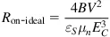
where εS is the dielectric constant of the semiconductor, μn is the electron mobility, and EC is the critical electric field for breakdown in the semiconductor. The denominator is called Baliga’s figure-of-merit (BFOM) [3,4]:
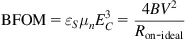
It is a measure of the power-handling capability (W/cm2) of a power device. Unipolar silicon carbide power devices have low on-state voltage drop due to its large BFOM. This is mainly due to the approximately tenfold increase in critical electric field for breakdown for SiC compared with silicon.
The ideal specific on-resistance for the drift region in 4H-SiC devices is compared with that for silicon in Fig. 1.3 for breakdown voltages from 100 to 100,000 V. A significant reduction in the specific on-resistance of drift regions is predicted by replacing silicon with 4H-SiC. The ratio of the specific on-resistance for silicon to that for 4H-SiC increases from 527 at a breakdown voltage of 100 V to 1280 for breakdown voltages above 40,000 V.

1.4 Silicon carbide power rectifiers
Silicon bipolar power P–i–N diodes operate with the injection of minority carriers during on-state current flow [2]. These carriers must be removed when switching the device from the on-state to the off-state. This is accomplished by the reverse recovery process that produces a large reverse current during turnoff. This current produces significant power losses in the diode and the switches in the circuits. It is therefore preferable to utilize unipolar current conduction in a power diode. The commonly used unipolar power diode structure is the Schottky rectifier that utilizes a metal-semiconductor barrier to produce current rectification. The high voltage Schottky rectifi...
Table of contents
- Cover image
- Title page
- Table of Contents
- Copyright
- List of Contributors
- Preface
- 1. Introduction
- 2. SiC material properties
- 3. Physical properties of gallium nitride and related III–V nitrides
- 4. SiC power device design and fabrication
- 5. GaN smart power devices and integrated circuits
- 6. GaN-on-GaN power device design and fabrication
- 7. Gate drivers for wide bandgap power devices
- 8. Applications of GaN power devices
- 9. Applications of SiC devices
- 10. Synopsys
- Index
Frequently asked questions
Yes, you can cancel anytime from the Subscription tab in your account settings on the Perlego website. Your subscription will stay active until the end of your current billing period. Learn how to cancel your subscription
No, books cannot be downloaded as external files, such as PDFs, for use outside of Perlego. However, you can download books within the Perlego app for offline reading on mobile or tablet. Learn how to download books offline
Perlego offers two plans: Essential and Complete
- Essential is ideal for learners and professionals who enjoy exploring a wide range of subjects. Access the Essential Library with 800,000+ trusted titles and best-sellers across business, personal growth, and the humanities. Includes unlimited reading time and Standard Read Aloud voice.
- Complete: Perfect for advanced learners and researchers needing full, unrestricted access. Unlock 1.5M+ books across hundreds of subjects, including academic and specialized titles. The Complete Plan also includes advanced features like Premium Read Aloud and Research Assistant.
We are an online textbook subscription service, where you can get access to an entire online library for less than the price of a single book per month. With over 1.5 million books across 990+ topics, we’ve got you covered! Learn about our mission
Look out for the read-aloud symbol on your next book to see if you can listen to it. The read-aloud tool reads text aloud for you, highlighting the text as it is being read. You can pause it, speed it up and slow it down. Learn more about Read Aloud
Yes! You can use the Perlego app on both iOS and Android devices to read anytime, anywhere — even offline. Perfect for commutes or when you’re on the go.
Please note we cannot support devices running on iOS 13 and Android 7 or earlier. Learn more about using the app
Please note we cannot support devices running on iOS 13 and Android 7 or earlier. Learn more about using the app
Yes, you can access Wide Bandgap Semiconductor Power Devices by B. Jayant Baliga in PDF and/or ePUB format, as well as other popular books in Technology & Engineering & Materials Science. We have over 1.5 million books available in our catalogue for you to explore.