- English
- ePUB (mobile friendly)
- Available on iOS & Android
eBook - ePub
Wide-band-gap Semiconductors
About this book
Wide-band-gap semiconductors have been a research topic for many decades. However, it is only in recent years that the promise for technological applications came to be realized; simultaneously an upsurge of experimental and theoretical activity in the field has been witnessed. Semiconductors with wide band gaps exhibit unique electronic and optical properties. Their low intrinsic carrier concentrations and high breakdown voltage allow high-temperature and high-power applications (diamond, SiC etc.). The short wavelength of band-to-band transitions allows emission in the green, blue, or even UV region of the spectrum (ZnSe, GaN, etc.). In addition, many of these materials have favorable mechanical and thermal characteristics.These proceedings reflect the exciting progress made in this field. Successful p-type doping of ZnSe has recently led to the fabrication of blue-green injection lasers in ZnSe; applications of short-wavelength light-emitting devices range from color displays to optical storage. In SiC, advances in growth techniques for bulk as well as epitaxial material have made the commercial production of high-temperature and high-frequency devices possible. For GaN, refinement of growth procedures and new ways of obtaining doped material have resulted in blue-light-emitting diodes and opened the road to the development of laser diodes. Finally, while the quality of artificial diamond is not yet high enough for electronic applications, the promise it holds in terms of unique material properties is encouraging intense activity in the field.This volume contains contributions from recognized experts presently working on different material systems in the field. The papers cover the theoretical, experimental and application-oriented aspects of this exciting topic.
Tools to learn more effectively

Saving Books

Keyword Search

Annotating Text

Listen to it instead
Information
Chapter 1
General reviews
Thin films and devices of diamond, silicon carbide and gallium nitride
Robert F. Davis , Department of Materials Science and Engineering, North Carolina State University, Raleigh, NC, USA
Robert F. Davis, Department of Materials Science and Engineering, North Carolina State University, Raleigh, NC 27607, USA.
The extreme properties of diamond, SiC and GaN provide combinations of attributes for high-power, -temperature, -frequency and optoelectronic applications. The methods of deposition, the results of chemical, structural, microstructural and electrical characterization and device development are reviewed for thin films of these three materials. Problems and areas of future research are also noted.
1 Introduction
The principal driving force for the current resurgence in interest in diamond (C), SiC and GaN (as well as cubic-BN, AlN, InN and alloys of these materials) is their potential as high-power, high-temperature microelectronic and/or optoelectronic devices resistant to radiation damage.
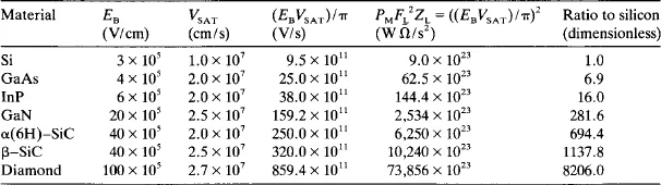
Johnson [1] has argued that the basic limitation on the high frequency and high power capabilities of selected discrete transistor devices is set by the product of the breakdown electric field, EB, and the saturated (limiting) electron velocity, Vs, i.e. the velocity at which an electron has enough energy to emit an optical phonon. Johnson’s figures of merit (EBVS/π)2 for selected semiconductors and their associated ratios to those for silicon are presented in table 1.
Table 1
Johnson’s figure of merit for a transistor’s power and frequency performance for selected semiconductor materials.
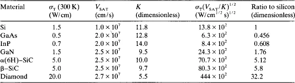
Keyes [2] has considered the switching speed of transistors in integrated circuits for computer logic applications. In this case a high limiting velocity allows high speed devices. A problem of small, closely spaced devices is the very high density of power dissipation, i.e. the production of heat. The heat flows from the device by conduction through the semiconductor material thereby encountering a thermal resistance that is inversely proportional to the size of the device. A lower limit is set on the device size by the maximum permissible thermal resistance and, thus, a high thermal conductivity, σT, is highly desirable in the device material. An additional set of figures of merit which includes Vs, σT and the dielectric constant K has been developed by Keyes [2] and is shown in table 2.
Table 2
Keyes’ figure of merit for the speed of a transistor for selected semiconductors.
Finally GaN and SiC are also of interest as light-emitting devices and for other optical applications. Important optical device applications for the nitrides include semiconductor lasers, light-emitting diodes (LEDs) and optical detectors. Although band-to-band transitions in SiC occur indirectly via intermediate energy levels in the conduction band and thus negate the possibility of laser applications, doping of the material with various donor and acceptor species allows electroluminescent devices to be produced. The creation of an abrupt p(aluminium doped)-n(nitrogen doped) junction in the α(6H)–SiC polytype (see discussion of polytypism in SiC in section 3) also allows the fabrication of blue LEDs in this form of SiC.
The following sections present an overview of the results and conclusions of recent materials research on diamond (diamond-like materials are not discussed), SiC and GaN as they pertain to microelectronics and optoelectronics, as well as a description of problems encountered and suggestions for future directions for research to overcome these problems.
2 Diamond
2.1 Background
The free energy difference between metastable diamond and stable graphite is only 453 cal/mol [3] at 1 atm. Thus the rarity of diamond is surprising when one considers that this is less than RT (≈600cal/mol) at room temperature. There are several reasons for the uncommon occurrence of diamond. Firstly, the kinetics of graphite formation are considerably faster than those of diamond, as would be predicted by the large activation energy barrier between these two materials [4]. Secondly, the entropy of diamond is less than the entropy of graphite by 0.78 cal/K mol [3]. Finally, a large activation energy barrier exists between graphite and diamond which prevents even small particles from forming at room temperature under equilibrium conditions. The density of diamond (3.51 g/cm3) is significantly greater than the density of graphite (2.25 g/cm3); thus, the former becomes the equilibrium form of C only at high pressure.
The breakthrough in the low-pressure synthesis of diamond was mainly a result of research by Soviet scientists in the late 1970s and early 1980s which indicated that gas activation techniques could greatly increase the growth rate of diamond while suppressing the graphite deposition. The results of these efforts clearly demonstrated that a concentration of atomic hydrogen, exceeding that of the equilibrium concentration associated with the thermal disassociation of the reactant hydrocarbon gas(es), was necessary to achieve diamond growth [5]. The flow of the hydrocarbon gas and hydrogen could now be simultaneous. In 1977, Derjaguin and Fedoseev [6] described three approaches to produce higher concentrations of atomic hydrogen than obtained previously: catalytic, electrical discharge and via heated tungsten filament. The significant results of this research were not published in English until 1981 [7] with additional details in 1984 [8]. This was followed by intensive efforts throughout the 1980s at the National Institute for Research in Inorganic Materials in Japan. This research quickly resulted in numerous publications [9–15] containing scanning electron micrographs of highly faceted, thick continuous films, confirming electron diffraction results and a host of spectroscopic data which removed all doubt that diamond films containing very small amounts of graphite could be grown at reasonable rates under highly metastable conditions on a variety of substrates, including Si, SiC, WC, Ta, W, Si3N4, Cu, Ni, Mo, BN, SiO2, Ti, Hf, Nb and Al2O3. This work also resulted in several new techniques for gas activation and diamond deposition. These have been grouped into five major categories [16]: (i) thermally activated chemical vapor deposition (CVD); (ii) high-frequency plasma enhanced CVD; (iii) direct-current (DC) discharge assisted CVD; (iv) combustion flame; and (v) hybrids of these and others. Only (i), (ii) and (iii) are considered likely to result in films suitable for electronic applications. Common to all techniques is the production of a high supersaturation of atomic H with a supersaturation of carbonic species and a substrate temperature in the range of 975–1275 K. Other similarities include process parameters of gas pressure (∼0.1 atm), the percentage of hydrogen in the gas phase (∼95–99.9%) and the resulting film morphology.
2.2 Nucleation and growth
2.2.1 The role of atomic hydrogen
One of the most important aspects of any discussion of the mechanisms and theory of diamond growth from the vapor phase is the role of atomic H. Firstly, within all the successful growth schemes which use H2 and a C-containing gas mixture for vapor phase deposition. The CH4 (or other hydrocarbon) and H2 are excited and dissociate into atomic H, hydrocarbon radicals and, in the case of plasma deposition, ions. The hydrocarbon species then adsorb onto the surface of the substrate and begin to grow via various hy...
Table of contents
- Cover image
- Title page
- Table of Contents
- Copyright
- Conference photograph
- Preface
- Introduction
- Chapter 1: General reviews
- Chapter 2: Growth
- Chapter 3: Doping
- Chapter 4: Defects and impurities
- Chapter 5: Characterization
- Chapter 6: Atomic and electronic structure
- Chapter 7: Devices
- Chapter 8: Surface, interfaces and quantum structures
- Chapter 9: New phenomena
- List of contributors
- Subject index
Frequently asked questions
Yes, you can cancel anytime from the Subscription tab in your account settings on the Perlego website. Your subscription will stay active until the end of your current billing period. Learn how to cancel your subscription
No, books cannot be downloaded as external files, such as PDFs, for use outside of Perlego. However, you can download books within the Perlego app for offline reading on mobile or tablet. Learn how to download books offline
Perlego offers two plans: Essential and Complete
- Essential is ideal for learners and professionals who enjoy exploring a wide range of subjects. Access the Essential Library with 800,000+ trusted titles and best-sellers across business, personal growth, and the humanities. Includes unlimited reading time and Standard Read Aloud voice.
- Complete: Perfect for advanced learners and researchers needing full, unrestricted access. Unlock 1.4M+ books across hundreds of subjects, including academic and specialized titles. The Complete Plan also includes advanced features like Premium Read Aloud and Research Assistant.
We are an online textbook subscription service, where you can get access to an entire online library for less than the price of a single book per month. With over 1 million books across 990+ topics, we’ve got you covered! Learn about our mission
Look out for the read-aloud symbol on your next book to see if you can listen to it. The read-aloud tool reads text aloud for you, highlighting the text as it is being read. You can pause it, speed it up and slow it down. Learn more about Read Aloud
Yes! You can use the Perlego app on both iOS and Android devices to read anytime, anywhere — even offline. Perfect for commutes or when you’re on the go.
Please note we cannot support devices running on iOS 13 and Android 7 or earlier. Learn more about using the app
Please note we cannot support devices running on iOS 13 and Android 7 or earlier. Learn more about using the app
Yes, you can access Wide-band-gap Semiconductors by C.G. Van de Walle in PDF and/or ePUB format, as well as other popular books in Physical Sciences & Condensed Matter. We have over one million books available in our catalogue for you to explore.