eBook - ePub
Characterization of Semiconductor Heterostructures and Nanostructures
- 496 pages
- English
- ePUB (mobile friendly)
- Available on iOS & Android
eBook - ePub
Characterization of Semiconductor Heterostructures and Nanostructures
About this book
In the last couple of decades, high-performance electronic and optoelectronic devices based on semiconductor heterostructures have been required to obtain increasingly strict and well-defined performances, needing a detailed control, at the atomic level, of the structural composition of the buried interfaces. This goal has been achieved by an improvement of the epitaxial growth techniques and by the parallel use of increasingly sophisticated characterization techniques and of refined theoretical models based on ab initio approaches. This book deals with description of both characterization techniques and theoretical models needed to understand and predict the structural and electronic properties of semiconductor heterostructures and nanostructures.
- Comprehensive collection of the most powerful characterization techniques for semiconductor heterostructures and nanostructures
- Most of the chapters are authored by scientists that are among the top 10 worldwide in publication ranking of the specific field
- Each chapter starts with a didactic introduction on the technique
- The second part of each chapter deals with a selection of top examples highlighting the power of the specific technique to analyze the properties of semiconductors
Trusted by 375,005 students
Access to over 1.5 million titles for a fair monthly price.
Study more efficiently using our study tools.
Information
Topic
Physical SciencesSubtopic
Analytic Chemistry1 Introduction: the interdisciplinary nature of nanotechnology and its need to exploit frontier characterization techniques
Abstract
High-performance electronic and optoelectronic devices based on semiconductor heterostructures are required to obtain increasingly strict and well-defined performances, needing a detailed control, at the atomic level, of the structural composition of the buried interfaces. This goal has been achieved by an improvement in the epitaxial growth techniques and by the parallel use of increasingly sophisticated characterization techniques and of increasingly accurate ab initio calculations. This chapter, introducing the book Characterization of Semi-conductor Heterostructures and Nanostructures, is divided into five sections. In \Section 1, the impact of nanoscience and nanotechnology in our society is described, using the point of view of the articles, the citations and the journals devoted to the field. The multidisciplinary nature of nanotechnology is reported in \Section 2, while the dynamic interplay among growth/synthesis techniques, theoretical modeling, and characterization techniques in the design and improvement of semiconductor heterostructure-based devices is discussed in \Section 3. \Section 4 reports the purposes of the book and the layout of the chapters. Finally, in \Section 5, the strength of combined experimental and theoretical investigation of a selected nanomaterial is underlined by an example.
Keywords
nanotechnology • nanoscience • heterostructures • nanostructures • characterization techniques • ab initio calculations
1 The scientific and editorial blow up of nanotechnology in the new millennium
The term nanotechnology refers to a branch of applied science and technology whose unifying theme is the control of matter at the atomic and molecular scale, normally 1–100 nm (1 nm = 10−9m), and the fabrication of devices within that size range. The appeal in such approach lies in the fact that the structural, physical, chemical, electronic, optical, etc. properties of nanometer-dimensioned materials differ markedly from those of the corresponding bulk (unconfined) materials. Nanotechnology, among the most advanced frontiers of Science, is certainly showing the higher degree of multidisciplinarity, generated from the well-accorded interplay among different fields such as materials science, applied physics, interface and colloid science, device physics, supramolecular chemistry, surface science, and engineering. Nanotechnology results from a combined extension of such sciences into the nanoscale.
Scientists, politicians, media, and industries have much expectation concerning what new science, technology, and application may result from these lines of research. Such expectations have strongly stimulated the effort made in the previous years by university and industrial laboratories in the field of nanoscience and nanotechnology. A simple way to evaluate such effort is to look to the number of papers published per year that are found using nanochemistry OR nanophysics OR nanotechnology OR nanoscience as search keys (\Fig. 1(a)), and to the number of citations that such papers have received (\Fig. 1(b)). It is evident that such simple and superficial statistical study is far to be comprehensive, as most of the papers that actually report results in this field do not necessarily used one of those four keywords. It is evident from the last row of \Table 1 that the 32 journals belonging to the Subject Category\1 named “Nanoscience & Nanotechnology” have published 8939 papers in 2006, while only 1125 have been found using those four keywords (\Fig. 1(a)). So, the data reported in \Fig. 1 are not important as absolute values, which are underestimated by a factor of about 10, but for the trend they are showing. It is evident that this trend shows an impressive acceleration starting from the new millennium.
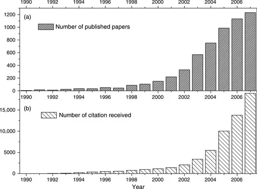
Fig. 1 (a) Number of paper published per year found using nanochemistry OR nanophysics OR nanotechnology OR nanoscience as search keys. Spanned period 1990 to 2007; total number of papers 5788 source ISI web of science. (b) Number of citations received per year by the papers reviewed in (a): total number of citations 59,747.
Table 1 List of a selection of scientific journals belonging to the Subject Category named “Nanoscience & Nanotechnology” sorted by publishing age. The last column refer to the aggregated values obtained by the 32 journals together. Data reported in this line allow to evaluate the impact of the Subject Category and to locate each single journal belonging to the category in a pondered ranking scale
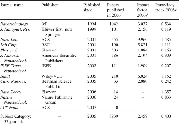
aThe journal impact factor of year 2006 is the average number of times articles from the journal published in 2005 and 2004 have been cited in 2006. Journals published first in 2006 will have their first impac...
Table of contents
- Cover image
- Title page
- Table of Contents
- Copyright
- Dedication
- Preface
- Chapter 1: Introduction: the interdisciplinary nature of nanotechnology and its need to exploit frontier characterization techniques
- Chapter 2: Ab initio studies of structural and electronic properties
- Chapter 3: Electrical characterization of nanostructures
- Chapter 4: Strain and composition determination in semiconducting heterostructures by high-resolution X-ray diffraction
- Chapter 5: Transmission electron microscopy techniques for imaging and compositional evaluation in semiconductor heterostructures
- Chapter 6: Accessing structural and electronic properties of semiconductor nanostructures via photoluminescence
- Chapter 7: Power-dependent cathodoluminescence in III–nitrides heterostructures: from internal field screening to controlled band-gap modulation
- Chapter 8: Raman spectroscopy
- Chapter 9: X-ray absorption fine structure in the study of semiconductor heterostructures and nanostructures
- Chapter 10: Nanostructures in the light of synchrotron radiation: surface-sensitive X-ray techniques and anomalous scattering
- Chapter 11: Grazing incidence diffraction anomalous fine structure in the study of structural properties of nanostructures
- Chapter 12: The role of photoemission spectroscopies in heterojunction research
- Chapter 13: ESR of interfaces and nanolayers in semiconductor heterostructures
- Subject Index
Frequently asked questions
Yes, you can cancel anytime from the Subscription tab in your account settings on the Perlego website. Your subscription will stay active until the end of your current billing period. Learn how to cancel your subscription
No, books cannot be downloaded as external files, such as PDFs, for use outside of Perlego. However, you can download books within the Perlego app for offline reading on mobile or tablet. Learn how to download books offline
Perlego offers two plans: Essential and Complete
- Essential is ideal for learners and professionals who enjoy exploring a wide range of subjects. Access the Essential Library with 800,000+ trusted titles and best-sellers across business, personal growth, and the humanities. Includes unlimited reading time and Standard Read Aloud voice.
- Complete: Perfect for advanced learners and researchers needing full, unrestricted access. Unlock 1.5M+ books across hundreds of subjects, including academic and specialized titles. The Complete Plan also includes advanced features like Premium Read Aloud and Research Assistant.
We are an online textbook subscription service, where you can get access to an entire online library for less than the price of a single book per month. With over 1.5 million books across 990+ topics, we’ve got you covered! Learn about our mission
Look out for the read-aloud symbol on your next book to see if you can listen to it. The read-aloud tool reads text aloud for you, highlighting the text as it is being read. You can pause it, speed it up and slow it down. Learn more about Read Aloud
Yes! You can use the Perlego app on both iOS and Android devices to read anytime, anywhere — even offline. Perfect for commutes or when you’re on the go.
Please note we cannot support devices running on iOS 13 and Android 7 or earlier. Learn more about using the app
Please note we cannot support devices running on iOS 13 and Android 7 or earlier. Learn more about using the app
Yes, you can access Characterization of Semiconductor Heterostructures and Nanostructures by Giovanni Agostini,Carlo Lamberti in PDF and/or ePUB format, as well as other popular books in Physical Sciences & Analytic Chemistry. We have over 1.5 million books available in our catalogue for you to explore.