1 Purity Requirements for Silicon in Photovoltaic Applications
Carlos del Cañizo Nadal, Simona Binetti, and Tonio Buonassisi
CONTENTS
1.1 Introduction
1.2 Back and Forth the Silicon Value Chain
1.2.1 Metallurgical Silicon Production
1.2.2 Ultra Purification of Silicon
1.2.3 Crystallization and Wafering
1.2.3.1 Monocrystalline Silicon for Solar Cells
1.2.3.2 Multicrystalline Silicon for Solar Cells
1.2.3.3 Direct Wafer Approaches for Solar Cells
1.2.3.4 Wafering
1.2.4 Solar Cell Processing
1.2.5 Purity Requirements as a Function of the Final Cell Performance
1.3 Quality Goals Depend on Cell Architecture
1.4 What Is Impacting Lifetime
1.4.1 Role of Dissolved Metal Contaminants
1.4.2 Metal Precipitation at Crystal Defects
1.4.3 Recombination Activity of Dislocations and Grain Boundaries
1.4.4 Dopant-Related Defects
1.4.4.1 B–O Pairs
1.4.4.2 H–P or H–B Complexes
1.4.4.3 Compensated UMG-Si
1.5 Integral Approach to Minimize Impurities and Defects throughout the Value Chain
1.6 Solar Silicon Definition
References
1.1 INTRODUCTION
Microelectronics measures its progress in terms of the number of transistors per chip, decrease in channel length, or supply voltage, but normally takes for granted the fact that it relies on the capability of silicon producers to purify silicon to extreme grades. Electronic-grade (EG) silicon, in fact, is a material of 99.9999999% (9N, i.e., nine nines), or even 99.999999999% (11N) purity, in a process that consumes hundreds of kWh per kg, and still needs further processing to grow crystalline ingots and slice them into wafers. This purity figure is exciting as it concerns a material with just one impurity atom every billion or hundred billion atoms, produced in an industrial environment. Microelectronics can afford the cost of this process because the share of the purification process cost in the final cost of a chip is insignificant, as it amounts to less than 0.5%, on the base of a rough estimate made by considering an annual market of 30,000 tons of silicon at US$50/kg, in a global microelectronics business of US$300 billion [1].
The photovoltaic (PV) industry, on the other hand, is strongly interested in a cheap silicon feedstock, as silicon represents around the 10%–15% of the total module cost [2,3,4]. In the race toward competitiveness in the energy market, PV aims at the cheapest pure silicon that does not compromise module performance.
This concern was present in the PV field from the early times of the technology, and special R&D efforts were made after the oil crisis of the 1970s, in particular in the United States through a large Department of Energy research program. Research was conducted under the general assumption that a purification process for the solar industry should not be as demanding as that for the semiconductor industry, in order that any reduction in the production cost could be worth it, even at the expense of a “dirtier” and “more-defective” material. A number of very different routes were followed, and a large amount of knowledge was accumulated in that period (see, e.g., [5,6] and Chapters 2 and 3 of this book).
But the progress of PV technology did not meet the expectations of the moment, PV was relegated to the funding priorities of the R&D supporting agencies, and no practical innovation in the Si-purification field was finally transferred to the PV industry, although some of the results were further applied for the semiconductor business [7].
The PV companies survived in the absence of a dedicated Si-purification process because their market was rather small, and they could benefit from the off-spec material and the idle capacity of the industry at reduced prices. The PV industry demanded around 3000 metric tons of purified silicon in 2000, to be compared to the 17,000 tons devoted to microelectronics [8]. However, the rapid growth of PV in the first 2000 decade quickly changed terms, increasing the demand of ultrapure silicon for PV to levels where the off-spec quantity or the extra-capacity was not enough. In 2006, the silicon demand for solar surpassed that for electronics for the first time, and by the end of the decade around 80% of the 100,000 tons produced by the industry were dedicated to the PV market [9]. Silicon suppliers were not able to attend the growing PV demand, so that a silicon shortage was experienced in the second half of the 2000s, with prices rocketing to the hundreds $/kg level. Moreover, when the silicon players, both incumbents and newcomers, finally reacted to provide the material demanded by the PV industry, the market did not grow as much as it was expected and the scenario quickly changed to that of oversupply. Prices fell dramatically to the $20/kg range. This price level presses silicon producers to further reduce their production costs if looking for a sustainable business [10,11], bringing to the forefront again the question of what is the optimum balance between purity requirements and process complexity.
1.2 BACK AND FORTH THE SILICON VALUE CHAIN
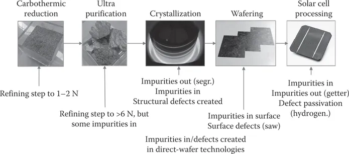
Producing ultrapure silicon is not the end of the hystory, as the material needs further processing to become a solar cell. This processing involves a number of high-temperature steps, not only with the potential incorporation of contaminants, but also with the opportunity to rearrange the impurities already there. Another aspect that should be considered as “part of the purity” is the presence of structural defects, which break the perfect covalent-bonded arrangement of the semiconductor atoms and interact with the impurities and charge carriers.
The solar-grade (SoG) quality, therefore, is the final result of a series of process steps, and to define a SoG quality one has to take into account the role of each process step (i.e., of the value chain of crystalline silicon PV technology) on the final quality of the material, not simply the residual impurity content, as done conventionally [5,12].
Figure 1.1 reports schematically the value chain of crystalline silicon PV technology, from quartz to the solar cell, indicating the main effects in terms of contamination, purification, and defect creation. Note that the interconnection and encapsulation of cells in a PV module are not included, as they typically involve much lower temperatures that do not appreciably change the impurity content and distribution in the solar cell.*
A brief description of each step is reported in what follows.
TABLE 1.1
Typical Impurity Concentration Ranges in Metallurgical Silicon
Impurity | Concentration Range in ppm(w) |
C | 50–1500 |
O | 100–5000 |
Total metals | 300–30,000 |
P | 5–100 |
B | 5–70 |
Source: Adapted from P. Hacke et al., 2010. IEEE Photovoltaic Specialist Conference, pp. 244–250.
1.2.1 Metatturgicat Sltlcon Production
Metallurgical silicon (MG-Si) is the raw material for pure silicon production. It comes from the carbothermic reduction of quartz at high temperature (~2000°C) in an electrical arc furnace (see Chapter 2 for details). Liquid silicon is produced, refined in a ladle, poured in a mold where it solidifies, and crushed. It contains from 1% to 3% of impurities depending on the raw materials and the type of electrode [15].
The main impurities typically present are C, O, Fe, Al, Ca, Ti, Mg, B, and P, whose concentration range is reported in Table 1.1 [16]. A careful selection of raw materials can lower the impurity content.
1.2.2 Ultra Purification of Sltlcon
To purify MG-Si, a three-step process known as the “Siemens process” is conventionally performed. MG-Si reacts with hydrogen chloride in a fluidized-bed reactor to synthesize a volatile silicon chlorides mixture, from which the trichlorosilane (TCS) (see details in Chapter 5) can be fractionally distilled in a number of columns, and then deposited as solid silicon by chemical vapor deposition (CVD) on slim Si seed rods heated by the Joule effect. Purities in the range of 9–11N (99.9999999%–99.999999999%) are achieved but at the cost of high energy consumption (in the range of 100 kWh/kg) and low efficiency deposition (for each mole of TCS converted to solid Si in the C...