In the past ten years, heteroepitaxy has continued to increase in importance with the explosive growth of the electronics industry and the development of a myriad of heteroepitaxial devices for solid state lighting, green energy, displays, communications, and digital computing. Our ever-growing understanding of the basic physics and chemistry underlying heteroepitaxy, especially lattice relaxation and dislocation dynamic, has enabled an ever-increasing emphasis on metamorphic devices. To reflect this focus, two all-new chapters have been included in this new edition. One chapter addresses metamorphic buffer layers, and the other covers metamorphic devices. The remaining seven chapters have been revised extensively with new material on crystal symmetry and relationships, III-nitride materials, lattice relaxation physics and models, in-situ characterization, and reciprocal space maps.
eBook - ePub
Heteroepitaxy of Semiconductors
Theory, Growth, and Characterization, Second Edition
- 643 pages
- English
- ePUB (mobile friendly)
- Available on iOS & Android
eBook - ePub
Heteroepitaxy of Semiconductors
Theory, Growth, and Characterization, Second Edition
About this book
Trusted by 375,005 students
Access to over 1.5 million titles for a fair monthly price.
Study more efficiently using our study tools.
Information
1
Introduction
Modern semiconductor devices require materials with a diversity of lattice constants, thermal expansion coefficients, and even crystal orientation or structure. Some of these materials are shown in the “bandgap engineering” diagrams of Figures 1.1 and 1.2. Because of the wide range of semiconductor materials used in devices, and the limited choices of single-crystal substrates on which to fabricate them, their manufacture almost always requires lattice-mismatched heteroepitaxial growth.1 Initial efforts were concentrated on pseudomorphic growth,2 in which the epitaxial materials are coherently strained and absent of misfit dislocations. However, the requirement to avoid lattice relaxation places considerable restrictions on the choices of compositions and layer thicknesses.3 In general, the thickness mismatch product is restricted to less than ≄0.04 nm for individual layers within pseudomorphic structures.4 Mismatched epitaxy brings with it a host of challenges, including strain,5 misfit dislocations,2 and the associated threading dislocations that propagate through device regions,6 crystallographic tilt induced during relaxation,7 and the possible degradation of morphology due to three-dimensional nucleation8 or stress-induced surface roughening.9 Foremost among these problems is the density of threading dislocations, which can exceed 109 cm−2 and strongly influences the performance and reliability of devices utilizing the defected material.10
The benefits of metamorphic heteroepitaxy greatly outweigh the challenges outlined above, however. First, heteroepitaxy enables semiconductor devices of nearly any composition, without the need for the identification of suitable lattice-matched substrates. It is important to note that even in lattice-matched devices, such as (AlxGa1−x)0.52In0.48P light-emitting diodes on GaAs substrates,11 differences in thermal expansion coefficients as well as limitations in compositional control give rise to lattice mismatch and dislocations. Second, heteroepitaxy enables the fabrication of heterojunction devices, such as lasers, light-emitting diodes (LEDs), and high-electron-mobility transistors (HEMTs). Third, devices made from different semiconductors may be integrated onto the same wafer, as in multijunction solar cells12 or the integration of optoelectronics and very large-scale integrated (VLSI) circuits.
The purpose of this book is to describe the principles involved in the heteroepitaxy of semiconductors and give some important examples of its application to metamorphic devices. The following chapters review the properties of semiconductors, heteroepitaxial growth methods, surface and chemical considerations, mismatched heteroepitaxy and strain relaxation, characterization of heteroepitaxial layers, defect engineering approaches, and metamorphic devices.
The strain relaxation, dislocation dynamics, and defect densities in heteroepitaxial layers are strongly influenced by the lattice constants, elastic constants, thermal expansion behavior, dislocation energetics, and kinetics. Chapter 2 reviews fundamental properties of semiconductors that bear on these aspects of mismatched heteroepitaxy.
Many advancements in the field of heteroepitaxy would not have been possible without the development of the epitaxial growth techniques—molecular beam epitaxy (MBE) and metalorganic vapor phase epitaxy (MOVPE)—which are reviewed in Chapter 3. These methods afford tremendous flexibility and the ability to deposit thin layers and complex multilayered structures with precise control and excellent uniformity. In addition, the high-vacuum environment of MBE makes it possible to employ in situ characterization tools using electron and ion beams, which provide the crystal grower with immediate feedback, and improved control of the growth process. For these reasons, MBE and MOVPE have emerged as general-purpose tools for heteroepitaxial research and commercial production. Together, these two epitaxial growth methods account for virtually all production of compound semiconductor devices today.
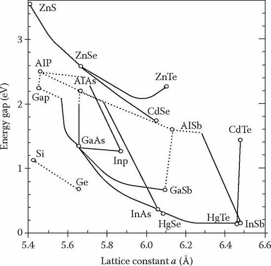
FIGURE 1.1
Energy gap as a function of lattice constant a for cubic semiconductors. Room temperature values are given. Dashed lines indicate an indirect gap.
Energy gap as a function of lattice constant a for cubic semiconductors. Room temperature values are given. Dashed lines indicate an indirect gap.
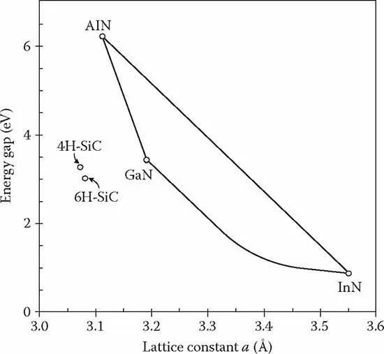
FIGURE 1.2
Energy gap as a function of lattice constant a for hexagonal semiconductors. Room temperature values are given. Sapphire, a commonly used substrate material for III-nitrides, has room temperature lattice constants of a = 4.7592 Å and c = 12.9916 Å. (From Y. V. Shvyd’ko et al., J. Synchrotron Rad., 9, 17, 2002.)
Energy gap as a function of lattice constant a for hexagonal semiconductors. Room temperature values are given. Sapphire, a commonly used substrate material for III-nitrides, has room temperature lattice constants of a = 4.7592 Å and c = 12.9916 Å. (From Y. V. Shvyd’ko et al., J. Synchrotron Rad., 9, 17, 2002.)
An important distinction between heteroepitaxy and homoepitaxy is the need to nucleate a new phase on the substrate surface. Therefore, the surface and its structure, as well as surface-segregated impurities (surfactants), can play important roles in determining the usefulness of heteroepitaxial layers for the fabrication of devices. Chapter 4 provides an in-depth description of semiconductor crystal surfaces and their reconstructions, nucleation, growth modes, and use of surfactants. Control of the growth mode, through the tailoring of growth conditions or the use of surfactants, is believed to be critical to the development of some devices. Two-dimensional growth is desirable in most cases, for the achievement of flat, abrupt interfaces and surfaces, and is mandated for quantum well devices. For the development of quantum dot devices, Volmer–Weber (island growth) or Stranski–Krastanov (growth of a continuous wetting layer followed by islanding) growth is actually desirable. Here, the control of the sizes, shapes, and distributions of islands is critical. This aspect, called the self-assembly of quantum dots, is also discussed in Chapter 4.
Heteroepitaxial growth is often metamorphic, so strain relaxation and the associated creation of crystal defects are of great importance. Under the condition of low lattice mismatch (<2%) it is possible to grow a pseudomorphic heteroepitaxial layer, which maintains coherency with the substrate crystal in the plane of the interface. At some thickness (the critical layer thickness), the creation of misfit dislocations becomes energetically favorable for relaxing the excess stress associated with the growth of mismatched materials. The lattice relaxation process is rather complex, and is usually limited by the nucleation, multiplication, glide, or climb of dislocations. Often, gliding dislocations are blocked by dislocations with orthogonal misfit components, depending on the strain and film thickness. Invariably, nonequilibrium threading dislocations are introduced, together with the stress-relieving misfit defects, and their concentration is determined by the aforementioned physical processes. The presence of dislocations in the material tends to degrade its electronic properties, affecting device performance and lifetime. The control of the lattice relaxation process is therefore an area of considerable interest. Chapter 5 provides an in-depth review of mismatched heteroepitaxy and lattice relaxation in uniform layers, while Chapter 6 considers graded and multilayered structures.
Characterization tools have played a key role in the advancement of the science of heteroepitaxy. Some of the most commonly used techniques are microscopic techniques, x-ray diffraction, photoluminescence, and crystallographic etching. These are covered in detail in Chapter 7, with an emphasis on x-ray diffraction, which is the most widely used nondestructive tool for structural characterization of heteroepitaxial layers. Individual sections are also devoted to some key application areas for these characterization tools, such as the determination of the stress, strain, and composition; the determination of the critical layer thickness for lattice relaxation; the characterization of the morphology and growth mode; the observation of crystal defects; and the determination of their types and configurations.
The broad application of mismatched heteroepitaxy to device and circuit fabrication requires the control of the crystal defect structures, and therefore a number of defect engineering approaches have emerged. Of these, buffer layer approaches have been broadly applied and are discussed in detail in Chapter 6. Chapter 8 reviews other defect engineering approaches, including reduced area growth, dislocation compensation, patterning and annealing, epitaxial lateral overgrowth (ELO), nanoheteroepitaxy, and compliant substrates. All of these were designed to reduce the dislocation densities of heteroepitaxial layers to practical levels for device applications. Some are intended to remove existing defects from lattice-relaxed heteroepitaxial layers, such as patterning and annealing, ELO, or superlattice buffer layers (dislocation filters). Others were conceived in order to prevent lattice relaxation in the first place; these include reduced area growth, nanoheteroepitaxy, and compliant substrates.
The proliferation of defect engineering methods could be taken as an indication that none of them are uniquely suited to the purpose, for all material systems. On the other hand, some of these approaches have been highly successful, to the point of being used in commercial devices. Graded buffer layers are the most important example of this, and have been used in commercial GaAs1−xPx LEDs on GaAs substrates and InxGa1−xAs HEMTs on GaAs substrates. ELO is an important method used to reduce the threading dislocation densities in the active regions of III-nitride lasers. Other defect engineering approaches, such as the use of compliant substrates, show great promise but have not yet found commercial use. In order to tap the great potential of heteroepitaxy, defect engineering approaches will continue to be important, not only in the applications listed above but also in new ones.
Chapter 9 discusses some of the important applications of metamorphic materials to semiconductor devices, including strain-relaxed buffer (SRB) metal oxide semiconductor field effect transistors (MOSFETs), HEMTs, LEDs, and solar cells. This list, though not exhaustive, provides a good cross section of applications and illustrates the relationships between processing, defects, strain, and surface roughness, and device characteristics. The rapid progress in the development of metamorphic devices can be expected to continue and, in fact, accelerate, based on the great success already achieved in this area.
References
1. E. A. Fitzgerald, A. Y. Kim, M. T. Currie, T. A. Langdo, G. Taraschi, and M. T. Bulsara, Dislocation dynamics in relaxed graded composition semiconductors, Mater. Sci. Eng., B67, 53 (1999).
2. J. W. Matthews and A. E. Blakeslee, Defects in epitaxial multilayers. I. Misfit dislocations, J. Cryst. Growth, 27, 118 (1974).
3. W. E. Hoke, T. D. Kennedy, A. Torabi, C. S. Whelan, P. F. Marsh, R. E. Leoni, S. M. Lardizabal, et al., Properties of metamorphic materials and device structures on GaAs substrates, J. Cryst. Growth, 251, 804 (2003).
4. L. J. Mawst, J. D. Kirch, C.-C. Chang, T. Kim, T. Garrod, D. Botez, S. Ruder, ...
Table of contents
- Cover
- Half Title
- Title Page
- Copyright Page
- Table of Contents
- Preface to the Second Edition
- Preface to the First Edition
- 1. Introduction
- 2. Properties of Semiconductors
- 3. Heteroepitaxial Growth
- 4. Surface and Chemical Considerations in Heteroepitaxy
- 5. Mismatched Heteroepitaxial Growth and Strain Relaxation: I. Uniform Layers
- 6. Mismatched Heteroepitaxial Growth and Strain Relaxation: II. Graded Layers and Multilayered Structures
- 7. Characterization of Heteroepitaxial Layers
- 8. Defect Engineering in Heteroepitaxial Material
- 9. Metamorphic Devices
- Appendix I
- Appendix II
- Appendix III
- Appendix IV
- Appendix V
- Appendix VI
- Appendix VII
- Appendix VIII
- Index
Frequently asked questions
Yes, you can cancel anytime from the Subscription tab in your account settings on the Perlego website. Your subscription will stay active until the end of your current billing period. Learn how to cancel your subscription
No, books cannot be downloaded as external files, such as PDFs, for use outside of Perlego. However, you can download books within the Perlego app for offline reading on mobile or tablet. Learn how to download books offline
Perlego offers two plans: Essential and Complete
- Essential is ideal for learners and professionals who enjoy exploring a wide range of subjects. Access the Essential Library with 800,000+ trusted titles and best-sellers across business, personal growth, and the humanities. Includes unlimited reading time and Standard Read Aloud voice.
- Complete: Perfect for advanced learners and researchers needing full, unrestricted access. Unlock 1.5M+ books across hundreds of subjects, including academic and specialized titles. The Complete Plan also includes advanced features like Premium Read Aloud and Research Assistant.
We are an online textbook subscription service, where you can get access to an entire online library for less than the price of a single book per month. With over 1.5 million books across 990+ topics, we’ve got you covered! Learn about our mission
Look out for the read-aloud symbol on your next book to see if you can listen to it. The read-aloud tool reads text aloud for you, highlighting the text as it is being read. You can pause it, speed it up and slow it down. Learn more about Read Aloud
Yes! You can use the Perlego app on both iOS and Android devices to read anytime, anywhere — even offline. Perfect for commutes or when you’re on the go.
Please note we cannot support devices running on iOS 13 and Android 7 or earlier. Learn more about using the app
Please note we cannot support devices running on iOS 13 and Android 7 or earlier. Learn more about using the app
Yes, you can access Heteroepitaxy of Semiconductors by John E. Ayers,Tedi Kujofsa,Paul Rago,Johanna Raphael in PDF and/or ePUB format, as well as other popular books in Technology & Engineering & Electrical Engineering & Telecommunications. We have over 1.5 million books available in our catalogue for you to explore.