- 288 pages
- English
- ePUB (mobile friendly)
- Available on iOS & Android
eBook - ePub
Fet Technology and Application
About this book
This book provides the reader with some insights into the many styles of field effect transistors (FETs) being used. It offers a rudimentary understanding of their operation and performance. The book explains the complex terminology that defines the various FET parameters.
Tools to learn more effectively

Saving Books

Keyword Search

Annotating Text

Listen to it instead
Information
1
Identifying the Family of FETs
1.1 Introduction
This chapter introduces the reader to all the field-effect transistors, or FETs, that we cover in this book; in addition, it offers a rudimentary, phenomenological understanding of how FETs operate.
Despite the plethora of both small-signal and power FETs, there are only two basic modes of operation. These operational modes are called the depletion mode and the enhancement mode.
Depletion-mode FETs are those whose drain current is reduced, or depleted, by the application of a gate potential whose polarity is opposite that of the drain voltage. Conversely, the enhancement-mode FET offers an increasing drain current when the polarity of the gate potential matches that of the drain voltage.
Within the family of FETs, shown in Figure 1.1, we have two major classifications: the junction FET, more commonly called the JFET, and the metal-oxide-semiconductor field-effect transistor, more commonly called a MOSFET. The JFET is classified as a depletion - mode FET, whereas the MOSFET can be designed to operate as either a depletion-mode or an enhancement-mode FET.
We could continue to embellish Figure 1.1, showing the many variants possible with both JFETs and MOSFETs, but we will not. Instead, this chapter offers brief descriptions and identifies where each best fits into the classification.
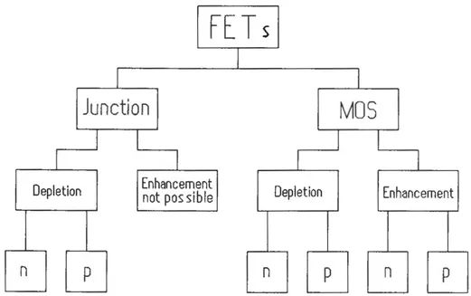
Figure 1.1 The family of FETs showing the two major classifications. Note that a JFET cannot operate in the enhancement region.
Before we continue, we need to be aware that a depletion mode MOSFET can frequently act and perform as an enhancement-mode MOSFET, but the enhancement-mode MOSFET cannot operate as a depletion-mode MOSFET.
There are several semiconductor materials suitable for the manufacture of FETs. For example, silicon, germanium, and gallium arsenide have been, or are being used. This text considers only FETs manufactured from silicon. No FETs are made using germanium.
1.2 Small-Signal JFETs
The basic operating principle of depletion-mode JFETs may be easily understood if we first review how the depletion fields are manipulated in a p-n diode.
1.2.1 Principles of p-n Diode Operation
The simple p-n junction diode, depicted in Figure 1.2, consists of a reasonably abrupt transition from p- to n-type semiconductor. This transition is brought about, to a great extent by the nature of the doping process as well as by the procedure used in fabrication. The p-reglon, called the acceptor, may be boron-doped semiconductor, whereas the n-region, called the donor, may be either arsenic or phosphorus-doped semiconductor.
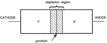
Figure 1.2 The simple pn junction showing the potential-barrier (depletion) region resulting from the interactions of electron and holes immediately adjacent to the interface.
In the p-region we have a lack of free electrons, whereas in the n-region there is an abundance. If we were to consider the valence of the boron-doped (p) silicon atom, we would notice that electrons are missing from the outer shell. We identify the locations at which no electrons exist in the outer orbit as holes. Conversely, an arsenic or phosphorus-doped (n) silicon atom has an excess of free electrons.
Immediately about the p-n interface of the junction diode the free electrons in the n-region jump the transition, filling the available holes in the p-region. The resulting regions in the immediate proximity of the interface become depleted of free carriers. The p-region is depleted of hole carriers; the n-region, depleted of electron carriers. This region bordering the p-n interface is identified as the depletion region. This n-to-p barrier "jumping" does not continue indefinitely, or until no free electron carriers exist. A counteracting electric field, called the Fermi level, quickly brings the reaction into equilibrium, halting further excursions of n-electrons into the p-region.
The Depletion Region
Carriers generally do not move across or through depletion regions. As the name implies, a depletion region is depleted of carriers (whether the carriers be electrons [n] or holes [p] necessary for conduction). How these depletion regions are manipulated in the p-n diode forms the substance of how a JFET operates.
At the p-n interface this potential-energy barrier or depletion region exists in both the p- and n-doped regions. The extent of the depletion region is dependent on the concentration of holes within the p-region as well as electrons within the n-region. Where the lesser concentration is, we will find the greater depletion area. Consequently, we find that the depletion ratio across the p-n interface is a function of the ratio of the doping densities.
For the typical p-n silicon diode this potential-energy barrier amounts to approximately 0.6 V. This means that to force carriers to jump the gap, we need to impress at least 0.6 of a volt (Vbi) of forward bias across the pn junction (viz., + on the p, or anode; — on the n, or cathode).
1.2.2 The Analogy to JFET Performance
All JFETs base their operation on the movement of the depletion field.
What happens if we apply a potential across the p-n diode in such a manner as to reverse-bias the junction? Remembering that like charges repel and unlike charges attract, we would expect all free carriers, whether they be holes (acting as positive charges) or electrons (which are negative charges), to be influenced according to this fundamental law. That is, negative charges would be attracted to a positive potential; positive charges to a negative potential. The result would be a greatly enlarged depletion region, as shown in Figure 1.3.
This depletion width may be calculated using a derivative of Poisson's equation.
where
vbi = "built-in" junction potential
VGS = applied bias
Kl = constant
Nc = carrier concentration
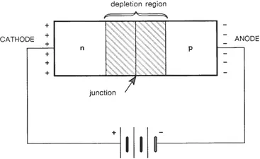
Figure 1.3 The simple pn junction showing the expanded depletion region caused by reverse bias.
We can now merge our visualization of the p-n diode with that of the JFET by placing two electrodes across either the n-doped (for an n-channel JFET) or p-doped (for a p-channel JFET) region as shown in Figure 1.4.
Current conduction between these two electrodes, which we may interchangeably call "source" and "drain," is uninhibited aside from the resistivity of the channel of doped silicon.
In a JFET the channel conductance is decreased as we increase the width of the depletion region, which immediately suggests that VGS has direct control over channel conductance and thus over channel current. The effect of gate bias (VGS) is shown in Figure 1.5a.
Before we continue, we need to remember that we control a JFET with a reverse gate-bias potential. If we were to forward bias the gate beyond the natural potential-energy barrier voltage, we would see a marked and sudden increase in gate current, as shown in Figure 1. 5b.
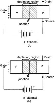
Figure 1.4 The rudi...
Table of contents
- Cover
- Half Title
- Series Page
- Title Page
- Copyright Page
- Preface
- Contents
- 1 Identifying the Family of FETs
- 2 How They Work: In a Layman's Language
- 3 Interpreting the Symbols
- 4 Characterization, Part I: How Parameters Are Achieved
- 5 Characterization, Part II: Parameter Action and Reaction
- 6 Thermal Relationships and Their Impact on Performancé
- 7 How to Read a Data Sheet and Understand What You are Reading
- 8 The Many Ways to Power Up FETs
- 9 Where Small-Signal FETs Are Found
- 10 Where Large-Signal FETs Are Found
- Symbol Index
- Index
Frequently asked questions
Yes, you can cancel anytime from the Subscription tab in your account settings on the Perlego website. Your subscription will stay active until the end of your current billing period. Learn how to cancel your subscription
No, books cannot be downloaded as external files, such as PDFs, for use outside of Perlego. However, you can download books within the Perlego app for offline reading on mobile or tablet. Learn how to download books offline
Perlego offers two plans: Essential and Complete
- Essential is ideal for learners and professionals who enjoy exploring a wide range of subjects. Access the Essential Library with 800,000+ trusted titles and best-sellers across business, personal growth, and the humanities. Includes unlimited reading time and Standard Read Aloud voice.
- Complete: Perfect for advanced learners and researchers needing full, unrestricted access. Unlock 1.4M+ books across hundreds of subjects, including academic and specialized titles. The Complete Plan also includes advanced features like Premium Read Aloud and Research Assistant.
We are an online textbook subscription service, where you can get access to an entire online library for less than the price of a single book per month. With over 1 million books across 990+ topics, we’ve got you covered! Learn about our mission
Look out for the read-aloud symbol on your next book to see if you can listen to it. The read-aloud tool reads text aloud for you, highlighting the text as it is being read. You can pause it, speed it up and slow it down. Learn more about Read Aloud
Yes! You can use the Perlego app on both iOS and Android devices to read anytime, anywhere — even offline. Perfect for commutes or when you’re on the go.
Please note we cannot support devices running on iOS 13 and Android 7 or earlier. Learn more about using the app
Please note we cannot support devices running on iOS 13 and Android 7 or earlier. Learn more about using the app
Yes, you can access Fet Technology and Application by E. S. Oxner in PDF and/or ePUB format, as well as other popular books in Physical Sciences & Physics. We have over one million books available in our catalogue for you to explore.