Photonic integrated circuit (PIC) technology holds great potential for breaking through the bottlenecks in current photonic and optoelectronic networks. Recently, a revolution has been witnessed in the field of lithium niobate (LN) photonics. Over the past decade, nanoscale LN waveguides with a propagation loss of ~0.01 dB and a radius of curvature on the level of ~100 ?m have been demonstrated. The revolution mainly benefits from two technological advancements, the maturity of lithium-niobate-on-insulator (LNOI) technology and the innovation of nanofabrication approaches of high-quality LNOI photonic structures. Using low-loss waveguides and high-quality-factor (high-Q) microresonators produced on the LNOI platform as building blocks, various integrated photonic devices have been demonstrated with unprecedented performances. The breakthroughs have reshaped the landscape of the LN industry.
This is the first monograph on LN nanophotonics enabled by the LNOI platform. It comprehensively reviews the development of fabrication technology, investigations on nonlinear optical processes, and demonstrations of electro-optical devices, as well as applications in quantum light sources, spectroscopy, sensing, and microwave-to-optical wave conversion. The book begins with an overview of the technological evolution of PICs, justifying the motivation for developing LNOI photonics. The next four chapters focus on LNOI photonics. The book concludes with a summary of the milestone achievements discussed in these chapters and provides a future perspective of this area of research.
Trusted by 375,005 students
Access to over 1.5 million titles for a fair monthly price.
Over the past half century, the advent and development of optical fiber communication technology has fostered a global optoelectronic network that has virtually allowed audio and/or video Communications between any individuals of nearly eight billion people anytime and anywhere. This miracle has created a unified human being society that represents an extremely complex system evolving into the largely unknown future. Within this system, those who can gather and process a large amount of information in a more efficient way can put themselves into a better position. The high demand in the ever-growing information transmission and processing rates call for the deployment of photonic integrated devices and systems into the fiber optic communication network. In addition, the photonic integrated circuits (PICs) have been considered as a potential technological platform for emerging applications such as big data, artificial intelligence, and quantum computation. In a nutshell, the transformation toward the next-generation information society requires photons to play the roles not only of information carriers but also of information processors.
Continuous effort has been dedicated to achieving large-scale photonic integration since the first proposal of the PIC concept in 1969 [52]. However, a standardized fabrication approach is yet to be identified and established. So far, several fabrication technologies have been demonstrated to enable realizing PICs consisting of moderate number of optical components, whereas each technology targets merely some specific academic and industrial applications and shows its pros and cons. More importantly, all the existing PIC technologies face enormous obstacles when aiming at the future ultralarge-scale photonic integration applications because the produced optical waveguides, an essential building block of PICs, cannot meet the three key requirements, including the low propagation loss, small bend radius, and high-refractive-index tuning efficiency at once.
Although a unified fabrication/manufacturing approach like the lithography manufacturing technology in the electronic integrated circuit (EIC) industry is still lacking in the field of photonic integration, significant achievements have been made along this direction by utilizing various material platforms. The detailed information can be found in a series of review articles [1, 8, 11, 13–16, 20, 28–30, 36, 37, 47, 49, 50, 54–56, 63, 64, 72, 79, 84]. For instance, three major PIC technology platforms based on fused silica, silicon/semiconductor, and lithium niobate have been reviewed in Refs. [1, 30, 36, 54, 63], [13–15, 20, 28, 29, 37, 55, 84], and [8, 11, 56, 64, 79], respectively. Thus, we figure out that instead of giving another comprehensive review on the traditional PIC technologies, lessons can be learned in a more enlightening way by comparing the characteristics and functionalities of the optical waveguides fabricated on different material platforms. This allows us to identify the strengths and weaknesses of the current major PIC technology platforms, thereby providing guidance for future investigations.
In general, optical waveguides are 1D photonic structures with a similar configuration and geometry as conventional optical fibers. Both the optical waveguide and the optical fiber have an inner layer of high refractive index (i.e., a core) surrounded by an outer layer of low refractive index (i.e., cladding). However, to construct photonic circuits, a number of optical waveguides need to be deployed on bulk substrates often with a spatial precision of merely a fraction of the wavelength. The substrate materials therefore must be transparent to light waves at operation wavelengths. The waveguides are produced on the substrates mainly by two strategies. One is to chemically modify the local refractive index in either the core or the cladding region; the other is to physically generate a ridge-like 1D structure on the substrate surface that acts as the waveguide core. Next, we show some representative examples achieved by the two fabrication strategies.
The concept of PICs, which is the photonic counterpart of the EICs invented in 1950s, was proposed by S. E. Miller in 1969 [52]. The two basic principles involved in Miller’s original idea of PICs are as follows. First of all, individual photonic components of various functionalities, such as light sources, light modulators, optical resonators, beam splitters and combiners, and filters, should all be designed and produced on the basis of planar optical waveguides. Second, planar waveguides and the further generated photonic circuits should be fabricated on bulk substrates using scalable lithographic technologies. Until now, the principles are still abided by the PIC community.
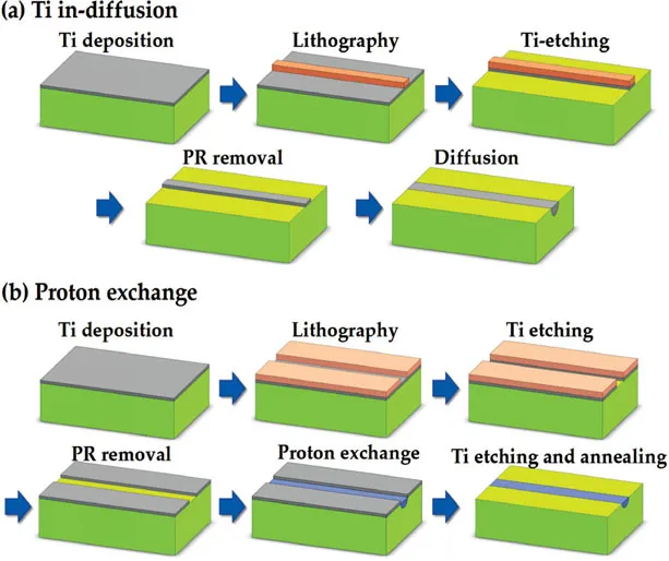
Soon after the proposal of PIC technology, the envisaged planar optical waveguides were successfully created on a crystalline lithium niobite (LN) substrate by space-selective modification of the composition in the core using various techniques, including out-diffusion, in-diffusion, and ion exchange techniques [5, 6, 11]. To understand the general properties of waveguides produced on the basis of the space-selective compositional modification in the core area, we illustrate the procedures of the titanium (Ti) in-diffusion technique in Fig. 1.1a as an example, because this fabrication technique has been in widespread use in the LN industry. First, a thin layer of Ti is uniformly deposited on the top surface of a piece of bulk LN crystal. Then, the metal layer is selectively removed using the lift-off lithographic technique to generate the waveguide pattern. The width of the metal strip is typically between 5 and 10 μm, depending on the operating wavelength in the waveguides. Diffusion of Ti into the LN crystal is realized by annealing the sample at high temperatures around 1000°C for durations ranging from a few to 10 hours. The Ti in-diffusion process leads to the doping of Ti in the crystalline LN, resulting in permanent refractive index changes on the order of 10−3 to 10−2. The Ti in-diffused LN waveguides have some significant advantages, including unspoiled electro-optic (EO) properties and strong light confinement for both transverse electric (TE) and transverse magnetic (TM) propagation modes, making them attractive for PIC applications demanding a high modulation rate, low propagation loss, and low polarization dependence.
Figure 1.1 Schematic of the representative fabrication techniques of lithium niobite (LN) waveguide: (a) titanium (Ti) in-diffusion and (b) proton exchange.
Alternatively, high-quality LN waveguides can also be achieved with proton exchange, as schematically illustrated in Fig. 1.1b. Likewise, photolithography is used to pattern the Ti film. However, this time it is the Ti overlapping the waveguide pattern that is selectively removed by the lift-off patterning. The lithographically defined LN specimen is then immersed in a liquid source of hydrogen at high temperature for replacing lithium ions by hydrogen ions, that is, protons. Proton exchange can generate a larger refractive index modification than Ti diffusion to enable stronger light confinement, whereas it is limited to the extraordinary refractive index. Both Ti-diffused and proton-exchanged LN waveguides have been used in telecommunication systems.
Aiming at the PIC application, the proton-exchanged LN waveguides have been used for constructing integrated quantum photonic circuits because crystalline LN, as a second-order nonlinear optical material, can be microengineered into periodically poled lithium niobate (PPLN) for realizing highly efficient phase-matched nonlinear processes, including harmonic generation and spontaneous parametric down-conversion (SPDC). The nonlinear optical properties lie at the heart of quantum information processing. In 2014, Jin et al. demonstrated the on-chip generation and manip...
Table of contents
Cover
Half Title
Title Page
Copyright Page
Dedication Page
Contents
Preface
1. Introduction
2. Fabrication Technology of Photonic Structures on Lithium-Niobate-on-Insulator
3. Nonlinear Optics in Nanostructures Fabricated on Lithium-Niobate-on-Insulator
4. Integrated Electro-Optic Devices on Lithium-Niobate-on-Insulator
5. Integrated Photonics on Lithium-Niobate-on-Insulator: Toward Real-World Applications
6. Summary and Future Perspectives
Index
Frequently asked questions
Yes, you can cancel anytime from the Subscription tab in your account settings on the Perlego website. Your subscription will stay active until the end of your current billing period. Learn how to cancel your subscription
No, books cannot be downloaded as external files, such as PDFs, for use outside of Perlego. However, you can download books within the Perlego app for offline reading on mobile or tablet. Learn how to download books offline
Perlego offers two plans: Essential and Complete
Essential is ideal for learners and professionals who enjoy exploring a wide range of subjects. Access the Essential Library with 800,000+ trusted titles and best-sellers across business, personal growth, and the humanities. Includes unlimited reading time and Standard Read Aloud voice.
Complete: Perfect for advanced learners and researchers needing full, unrestricted access. Unlock 1.5M+ books across hundreds of subjects, including academic and specialized titles. The Complete Plan also includes advanced features like Premium Read Aloud and Research Assistant.
Both plans are available with monthly, semester, or annual billing cycles.
We are an online textbook subscription service, where you can get access to an entire online library for less than the price of a single book per month. With over 1.5 million books across 990+ topics, we’ve got you covered! Learn about our mission
Look out for the read-aloud symbol on your next book to see if you can listen to it. The read-aloud tool reads text aloud for you, highlighting the text as it is being read. You can pause it, speed it up and slow it down. Learn more about Read Aloud
Yes! You can use the Perlego app on both iOS and Android devices to read anytime, anywhere — even offline. Perfect for commutes or when you’re on the go. Please note we cannot support devices running on iOS 13 and Android 7 or earlier. Learn more about using the app
Yes, you can access Lithium Niobate Nanophotonics by Ya Cheng in PDF and/or ePUB format, as well as other popular books in Technology & Engineering & Biology. We have over 1.5 million books available in our catalogue for you to explore.