Nanoscale materials and structures have attracted great attention in recent years because of their unique physical and chemical properties and potential use in energy transport and conversion. This book puts the subject into context by first looking at current synthesis methods for nanomaterials, from the bottom-up and top-down methods, followed by enhanced energy conversion efficiency at the nanoscale and then specific applications e.g. photovoltaic cells and nanogenerators. This authoritative and comprehensive book will be of interest to both the existing scientific community in this field, as well as for new people who wish to enter it.
Trusted by 375,005 students
Access to over 1.5 million titles for a fair monthly price.
National Laboratory of Solid State Microstructures and School of Electronic Science and Engineering, Nanjing University, Nanjing 210093, P. R. China *Email: [email protected]
1.1 Introduction to Graphene
Carbon is one of the most studied elements in the periodic table. The versatility of chemical bonds enables many carbon allotropes. In three-dimensional bulk form, carbon can exist as diamonds and graphite, which comprise of sp3 and sp2 covalent bonds, respectively. In the 1980s and 1990s, another two types of carbon allotropes, the zero-dimensional fullerene1 and one-dimensional carbon nanotubes,2 were discovered (Figure 1.1(a)).3 These nanomaterials, with fascinating physical and chemical properties, have driven an enormous amount of research in many areas.4 However, the two-dimensional counterpart of carbon allotrope was still missing until 2004, when a single layer of graphite, or graphene, was successfully isolated on a substrate.5 In this section, we give a brief introduction to graphene. We do not intend to derive the properties of graphene from the lattice and band structures. Readers who are interested in those aspects are encouraged to read the excellent reviews that are available.6,7
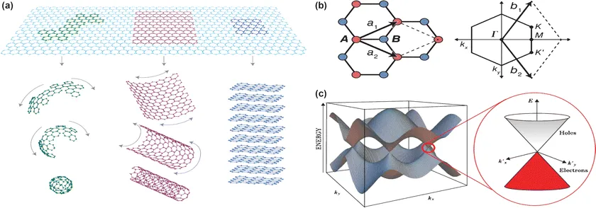
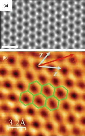
Figure 1.1 (a) Schematic drawing of the relationship between graphene and other carbon materials. Graphene is a 2D building material for carbon materials of all other dimensions. It can be wrapped up into 0D buckyballs, rolled into 1D nanotubes or stacked into 3D graphite. Adapted from Ref. 3. The lattice structure of graphene with the yellow region as the unit cell. (b) (Left) Hexagonal crystal structure of graphene with lattice parameters a1 and a2 and inequivalent atomic positions A and B of the diatomic basis shown in red and blue. (Right) Reciprocal lattice and Brillouin zone with reciprocal lattice parameters b1 and b2, showing Dirac points K and K′ at the Brillouin zone corners, as well as M, the midpoint of the BZ edge and Γ, the center of the Brillouin zone. Adapted from Ref. 90. (c) (Left) Electronic band structure of graphene. (Right) Enlargement of the band structure near the Dirac cone. Adapted from Ref. 91.
1.1.1 Lattice and Band Structure
Graphene is composed of a honeycomb lattice of carbon atoms (Figures 1.1(b) and 1.2). Structurally, graphene is related to many carbon allotropes. For example, carbon nanotubes can be formed by rolling graphene along certain axes, and graphite can be formed by stacking graphene vertically3 (Figure 1.1(a)). The structure can be seen as a triangular lattice with two equivalent atoms in each unit cell. The unit vectors
, where a=1.42Å is the carbon–carbon distance (Figure 1.1(b)). The reciprocal lattice is also triangular, with unit vectors
. The shape of the Brillouin zone is rotated 90° compared to the lattice unit cell. In each Brillouin zone, there are two inequivalent corners, K and K′, called Dirac points. This is related to the presence of a pseudospin degree of freedom or two independent sublattices in graphene.6,7
Figure 1.2 Lattice structure of graphene under (a) TEM and (b) STM showing the hexagonal lattice. Adapted from Refs. 92 and 93.
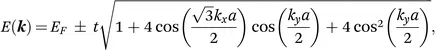
The tight-binding band structure of graphene was calculated in 1947 by Wallace,8 which can be described by eqn (1).
(1)
here EF is the Fermi energy, t is the nearest neighbor hopping integral. The±signs represent conduction and valance bands respectively. Figure 1(c) is the plot near the first Brillouin zone. The band structure of graphene is drastically different from that of conventional semiconductors. The most remarkable feature is the linear dispersion relation near the Dirac points, which resembles ultrarelativistic particles and can be described by the massless Dirac equation.6,7 Therefore, the electrons in graphene are often called massless Dirac fermions. This can be seen quantitatively by expanding eqn (1) near the Dirac points to give eqn (2).
E(k)=±hνFk(2)
where vF=3ta/2h is the graphene Fermi velocity. Take t=2.5 eV, vF≈108 cm s−1, about 1/300 of the speed of light.6 Due to the unique dispersion relation, the density of states of graphene is linear with energy and vanishes at the Dirac points. This is again in contrast to conventional 2D materials with a constant density of states. The unique band structure of graphene has led to many intriguing phenomena like half integer quantum Hall effect,9,10 Klein tunneling,11 and electron focusing.12
1.1.2 Properties and Potential Applications
Graphene has many unique electrical, optical, mechanical properties and potential applications, which make it one of the most studied materials in the past ten years. Below we summarize some of the physical properties and potential applications of graphene, many of which require the fabrication of nanostructures, which will be discussed later in the chapter.
1. High carrier mobility Electrons in graphene have well-defined chirality, which is related to the two component pseudospin degree of freedom. Such chirality prevents intervalley backscattering and therefore leads to intrinsically high mobility.6 Another advantage of graphene, compared to III-V semiconductors,13 is that the electron and hole mobility are equally high, due to the symmetric band structure. Theories have predicted that the phonon limited mobility can be as high as 2×105 cm2 Vs−1 at a carrier concentration of 1012 cm−2.14 A similar mobility value has already been measured experimentally.15,16 The ultrahigh mobility makes graphene a potential candidate in electronic applications, including radio frequency and logic transistors.3,17–19 Although the absence of a bandgap places a major obstacle for logic applications, many ways of opening a bandgap have been proposed and tested, which will be the focus of discussion in this chapter.
2. Conductive and transparent Due to the absence of backscattering, the resistivity of pristine graphene is expected to be ≈1×10⁻⁶ Ωcm, which is lower than the most conductive metal, silver, at room temperature.20 Optically, graphene is quite transparent over the visible spectra, absorbing 2.3% of the light. However, considering that graphene only has one atomic layer, such absorption is quite dramatic. The absorption is expressed by a simple formula πα, where α≈1/137 is the fine-structure constant.21 Such an optical feature originates from the unique conical band structure of graphene near the Dirac points. With a combination of high conductivity and transparency, graphene is expected to find applications in transparent conducting films.17 As a possible candidate to replace the increasingly costly indium tin oxide (ITO) based films, graphene is made entirely of carbon. Another advantage is the extreme mechanical strength and flexibility.22 Potential near term applications include touch screen display, e-paper and organic light-emitting diodes.17
3. Wide-band and tunable optical absorption Graphene has a tunable optical absorption. Since the density of states is vanishing at the Dirac points, the Fermi energy can be tuned by carrier density (normally through electrostatic gating). The Pauli blockade ensures that optical absorption is only possible for energy greater than 2EF.23 Therefore, graphene is expected to respond to wide-band signals spanning microwave to ultraviolet, including the commonly used fiber-optic communication band at 1.55 μm. Combined with the superior carrier mobility, possible applications include ultrafast photodetectors, modulators, terahertz wave detectors and tunable fiber mode-locked lasers.17,24
4. Large specific surface area Since every atom of graphene is on its surface, graphene has one of the largest specific surface areas among all materials, 2630 m2 g−1. Therefore graphene is expected to have applications in sensors: it has been shown that detection of single molecule is possible with graphene.25 Combined with high conductivity and transparency, graphene also has great potential in energy related applications. For example, supercapacitor electrodes require large conductivity for high specific power and large surface area for high specific energy. Chemically exfoliated graphene is shown to possess both properties and have superior capacitance.26,27 Another example is lithium ion batteries. Since (chemically-reduced) graphene has a higher conductivity and can accommodate more strain than many cathode materi...
Table of contents
Cover
Title
Copyright
Preface
Contents
Author Biographies
Chapter 1 Fabrication Techniques of Graphene Nanostructures
Chapter 2 Nanophotonic Light Trapping Theory for Photovoltaics
Chapter 3 Micro/nano Fabrication Technologies for Vibration-Based Energy Harvester
Chapter 4 Thermal and Thermoelectric Properties of Nanomaterials
Chapter 5 Nanotubes for Energy Storage
Chapter 6 Measurements of Photovoltaic Cells
Subject Index
Frequently asked questions
Yes, you can cancel anytime from the Subscription tab in your account settings on the Perlego website. Your subscription will stay active until the end of your current billing period. Learn how to cancel your subscription
No, books cannot be downloaded as external files, such as PDFs, for use outside of Perlego. However, you can download books within the Perlego app for offline reading on mobile or tablet. Learn how to download books offline
Perlego offers two plans: Essential and Complete
Essential is ideal for learners and professionals who enjoy exploring a wide range of subjects. Access the Essential Library with 800,000+ trusted titles and best-sellers across business, personal growth, and the humanities. Includes unlimited reading time and Standard Read Aloud voice.
Complete: Perfect for advanced learners and researchers needing full, unrestricted access. Unlock 1.5M+ books across hundreds of subjects, including academic and specialized titles. The Complete Plan also includes advanced features like Premium Read Aloud and Research Assistant.
Both plans are available with monthly, semester, or annual billing cycles.
We are an online textbook subscription service, where you can get access to an entire online library for less than the price of a single book per month. With over 1.5 million books across 990+ topics, we’ve got you covered! Learn about our mission
Look out for the read-aloud symbol on your next book to see if you can listen to it. The read-aloud tool reads text aloud for you, highlighting the text as it is being read. You can pause it, speed it up and slow it down. Learn more about Read Aloud
Yes! You can use the Perlego app on both iOS and Android devices to read anytime, anywhere — even offline. Perfect for commutes or when you’re on the go. Please note we cannot support devices running on iOS 13 and Android 7 or earlier. Learn more about using the app
Yes, you can access Nanofabrication and its Application in Renewable Energy by Gang Zhang, Navin Manjooran in PDF and/or ePUB format, as well as other popular books in Tecnología e ingeniería & Química. We have over 1.5 million books available in our catalogue for you to explore.