![]()
Chapter 1
ION IMPLANTATION FOR FABRICATION
OF SEMICONDUCTOR DEVICES AND MATERIALS
Michael I. Current
1729 Comstock Way, San Jose, CA 95124, USA
Ion acceleration of dopants and other ions is a critical and nearly universally employed tool for the fabrication of transistors in IC devices and the various forms of electronic, photovoltaic, and photonic materials. This chapter reviews the major types of accelerators, ions sources, and scanning methods used in contemporary practice for ion implantation for electronic, photo-voltaic, and biomedical applications.
1. Introduction
The use of accelerated ions to dope and modify semiconductor materials, generally called ion implantation, is a core technology for fabrication of integrated circuits (IC) that form the backbone of the global communications and advanced computation capabilities that have transformed modern life over the last half-century. The use of ion implanters in the IC industry, starting in the 1970s for precision doping of channel structures at doping densities of ~10−4 monolayers to set the threshold conditions for transistor switching, enabled the practical fabrication of complementary metal-oxide semiconductor (CMOS) transistors that are now the dominant form of IC devices. Development of accelerator technologies capable of delivering highly stable and collimated ion beam currents ranging from a few µA to 100 mA and incident ion energies ranging from 100 eV to ~10 MeV have provided a broad and capable technology for fabrication of ICs for logic, memory and analog operations as well as an increasingly varied array of optical sensors and imaging devices. Ion implantation is now used for the overwhelming majority of applications for doping of semiconductor materials and in an increasing array of applications for creation and modification of electronic and photonic materials.
The yearly revenues from the sale of industrial ion implantation and materials modification tools constitute a US$1.5B market (in “normal” economic environments). In addition, there are substantial markets for suppliers of dopant species materials (~US$140 M/year) and a diverse array of suppliers of spare and upgrade parts and services. Additional parts of the ion implantation commercial infrastructure include the suppliers of system components, magnets, power supplies, and vacuum pumps, and a varied array of metrology tools focused on process characterization and control applications.
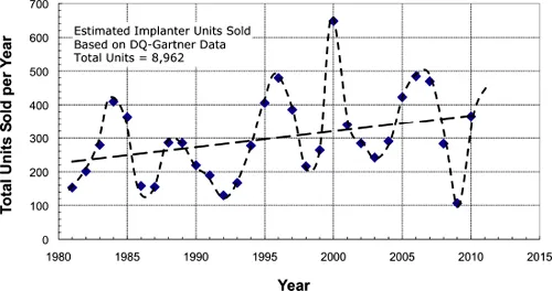
Fig.1. Estimates of the number of commercial ion implanters sold per year, mainly for IC fabrication. The data shown here are an underestimate, particularly for the earlier years.
The average number of commercial ion implantation systems sold per year, predominantly for fabrication of Si-based IC devices, has increased from ~250 to ~350 per year since 1980 as seen in Fig. 1. The year-to-year sales show large fluctuations due to the highly cyclic nature of IC fab construction trends especially when driven by additional factors, such as shifts in dominant wafer sizes, introduction of new implanter machine types and IC devices, expansion into new global regions, and variations driven by general economic cycles. The combination of these technology and market factors has resulted in a rather steady “5 year” cycle in units sold per year over the last 3 decades.
2. Applications of Ion Implantation: Devices and Materials
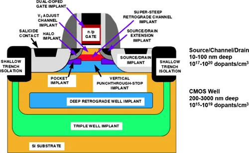
The planar CMOS transistor, illustrated in Fig. 2, has been the workhorse device structure for IC devices for logic and memory applications since the mid-1980s.
Fig. 2. Sketch of major doped regions for a planar CMOS transistor.
For doping of near-surface (<100nm) layers on Si with the common dopants B, As, and P, the beam energy requirements for atomic species is a fraction of a keV to a few tens of keV. Increasingly the ion species of choice for low energy (sub-keV) implants is some form of molecular ion containing up to 18 dopant atoms (for B18H22), allowing for beamline operation at proportionally higher energies and significantly higher total beam flux for higher production throughputs. For deeper profiles to form CMOS wells for transistors and optical imagers, ion energies range up to several MeV.
The initial applications for ion implantation were for low dose (1011 to 1012 ions/cm2) doping of CMOS channels to set the transistor switching, or “threshold”, conditions. These implants required relatively modest beam currents with 100 to 500 µA being common for “medium-current” implanters. By 1980, higher current sources and beam lines were developed for “high-current” machines to produce beams of 1 to 30 mA of dopant ions. These machines were capable of efficient implants with doses of ~5×10¹⁵ ions/cm2 used for CMOS source/drain junctions as well as emitter, buried layer, and collector implants for bipolar devices.
By the late 1980s, implantation machines capable of ion energies of ~1−2 MeV were being used for doping deep “retrograde” wells in CMOS devices to suppress latch-up instabilities between neighboring well structures and to reduce radiation-generated “soft failures” in DRAM arrays. With the evolution of complex doping schemes to suppress lateral punch-through between source and drain junctions in short channel (<100 nm) transistors, ion implanters were developed with capabilities for mid-1014 ions/cm2 doping at beam incidence angles up to 45° to provide additional well doping in a “halo” surrounding shallow source/drain extension (SDE) junctions.
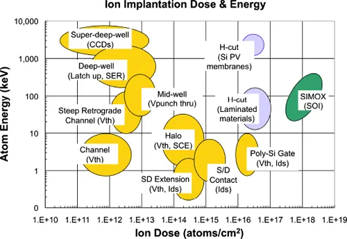
The dose range for implant doping expanded above 1016 ions/cm2 with the use of very high dose implants to counter-dope poly-Si gates in pMOS transistors in DRAM circuits. To reduce the overall processing cost, an n-doped poly-Si thin film was deposited over the entire wafer and used for the nMOS transistor gates. For the pMOS transistors, a very high dose (3−5 × 10¹⁶ B/cm2) implant was needed to counter-dope the n-type dopants and transform the pMOS gates into a highly-doped, p-type material. This led to the use of “plasma immersion” and “ion shower” types of doping tools, which were especially suited for very high dose implants at low (several keV and less) energies.
With the wide-spread use of Si-based imagers for cell-phone and other cameras, fabrication of charge-coupled devices (CCDs) and CMOS imagers called for the use of implanters with energy ranges of 2–8 MeV for formation of doped regions up to 4 µm deep. These dopant implants for CMOS devices, with many additional specialized applications for analog and bipolar components, fill in the space occupied by the left side and lower segments on the dose–energy chart shown in Fig. 3.
2.1. Pre-amorphization
In recent years the implantation of non-dopant ions (Ge, C, N, F, H, etc.) has become a standard part of the range of ion species in use for CMOS device fabrication. The most direct form of these applications is the implantation of Si or Ge ions at doses high enough (~1015 ions/cm2) to transform a surface layer of Si into an amorphous form through accumulation of lattice recoil damage during the stopping of the Si or Ge ions. The initial purpose of these “pre-doping amorphization implants” (PAI) was to eliminate the channeling of light ions, mainly B, in crystalline Si and to enable the formation of shallow dopant profiles with low-energy implants. While suppression of ion channeling effects is still important, the uses of PAI implants have broadened to include activation of dopants during Si re-crystallization growth in the low temperature (<700°C) furnace and microwave anneals.1 In addition, PAI implants are used to take advantage of the increased absorption of light in amorphous-Si layers during ms-timescale annealing with laser or flash lamp sources.
Fig. 3. Dose and atom energy regions for CMOS transistor doping, high dose hydrogen implants for Si layer splitting (H-cut), and direct implantation of oxygen to form SOI wafers (SIMOX).
PAI implants are also used for materials modification of poly-Si gates to boost the net strain in CMOS channel regions in order to improve carrier mobility and overall transistor drive currents. There are many variants of “stress memorization” techniques using PAI steps to amorphize poly-Si gate electrodes, resulting in an overall tensile strain (good for nMOS) in the transistor channel. The “remembered” channel strain levels are held in place in the final CMOS device through the replacement of the poly-Si with a metal gate electrode and addition of nitride overlayers.2
2.2. Cocktail implants
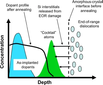
Non-dopant atoms, mainly C, F, and N (commonly referred to as “cocktail atoms”), are implanted as part of an implant-and-anneal sequence to control the diffusion of shallow dopant profiles through trapping of Si interstitials at the cocktail atom profile location.3 The process starts with a deep PAI implant (with Ge or Si) followed by the implantation of cocktail atoms at a mid-depth location and dopants near the surface (see Fig. 4). When this combination of implants is followed by a rapid thermal process (RTP) anneal at ~1050°C for ~1 s, the amorphous layer re-grows early in the anneal cycle into near-perfect crystalline Si, leaving a deep layer of defects at the end of-range (EOR). As the high-temperature cycle continues, the EOR damage anneals and releases Si interstitial atoms. If the shallow dopants are B or P, which diffuse rapidly when combined with enhanced concentrations of Si interstitials, then the presence of a Si interstitial trapping layer “starves” the dopant diffusion process resulting in shallower dopant profiles at the end of the RTP anneal cycle. These sorts of combination implants with dopant and non-dopant atoms can be used as a method to control dopant diffusion and fabricate activated shallow junctions with the use of RTP anneal equipment, forestalling the need to shift to more costly and complex ms-timescale anneals with lasers or flash lamps.
Fig. 4. Schematic diagram of the implant and damage profiles for the use of “cock-tail” atoms (C, F, N) to reduce the diffusion of dopants (B, P) that diffuse rapidly when combined with Si interstitials.
2.3.Carbon implants for tensile strained nMOS
Another use for C implants is to create local strain regions to establish tensile strain conditions (which increase electron mobilities in Si) in the channels of nMOS transistor...