![]()
CHAPTER 1
AN INTRODUCTION TO SEMICONDUCTOR MATERIALS
This chapter discusses the intentions of the book, the general properties and generation of X-rays, and the structural and chemical information that can be extracted through diffraction. Much of the emphasis is on composite layer structures, because of their technological importance. These layer structures create interesting challenges because of the stresses generated, which cause strains that can be very anisotropic. A detailed explanation is presented of the elasticity for all combinations of orientation and symmetry. Some of the basics of epitaxy are discussed and how with certain combinations of materials, complex microstructures can exist.
1.1. General outline
Semiconductor materials exist in many structural forms and therefore require a large range of experimental techniques for their analysis. The advantage of concentrating on this class of materials is that the amount of detailed structural information is impressive, however the application of the methods described is not exclusive to these material types. Scattering from powder samples will be covered theoretically and how a greater understanding of the scattering can give rise to extra information. The overall intention of this book though, is to allow the reader to obtain a good working knowledge of X-ray diffraction theory, techniques and analysis, so that he or she is fully aware of the possibilities, assumptions and limitations with this form of structural investigation.
The molecular structure of semiconductors is in general well known. Most materials of interest have been manufactured in some way; therefore an approximate knowledge of the elements and layer thicknesses and sequence is assumed, and is the starting point for many of the approaches used. Most samples of interest, however, are not of a simple molecular form but are composite structures, commonly consisting of multiple thin layers with different compositional phases. There are many important structural parameters that can modify semiconductor device performance. These parameters include phase composition, micro-structural or layer dimensions and imperfections, etc. A description of how the properties are categorised and material form is given, since this largely determines the X-ray scattering experiment for the analysis, Fewster (1996).
The theory of X-ray scattering is presented from a physical basis and therefore naturally starts with dynamical theory and its extensions before describing the more approximate kinematical theory. The theories are largely considered at the single photon level. In reality the experiment collects many photons that are divergent and occupy a range of energies. These effects influence the experimental results and are covered in the description of the instruments. In general the scattering is three-dimensional because the sample is three-dimensional and this is born in mind throughout. The mapping of the scattering in three-dimensions is the most general experiment and all other approaches are obvious projections. The assumptions on moving to two-dimensional reciprocal space mapping and ultimately one-dimensional X-ray scattering, e.g. rocking curves will then appear more obvious and understandable. The assumptions associated with interpreting data collected in various ways will be discussed. This will then allow the reader to understand the subject conceptually and extend the techniques to his or her particular problem.
The concentration is on near-perfect semiconductor materials, whose elements are defined by their valence in the Periodic Table, that is group IV, III-V, II-VI, etc., since the available information is large as well as being commercially very important. The concentration on near-perfect materials is to contain the range of techniques and available information. Although the techniques will be considered in general terms so as not to limit the book to specific materials. These near-perfect materials are essentially extended single crystals, however as the perfection declines they become more mosaic until eventually polycrystalline. Since this edition is more comprehensive and concentrates on the whole process of collecting data, including the diffraction process and the instrumental aberrations, this is extended to include polycrystalline material analysis and powder diffractometers.
Interpretation requires a good understanding of the instrument aberrations, the assumptions in the methods and presumed details concerning the sample. Aspects of quality control with X-ray diffraction methods based on comparative measurements requires an understanding of the sensitivity of the conditions to the parameters of interest, these aspects will also be covered.
1.2. Semiconductors
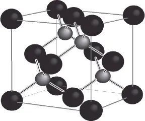
Semiconductors range from the most perfect crystals available to amorphous materials. The sample dimensions can range from 12 inch (although 18 inch is possible) diameter ingots of bulk Si, down to layers of partial-atomic coverage with nanometre scale lateral dimensions embedded in a multi-layer structure. The molecular structure of most common semiconductors is of a high symmetry extended lattice, for example Si has the space group (this represents the relative relationships between atoms) of Fd3m and the space group for GaAs and InP is F43m, whereas GaN in hexagonal form has the space group P63mc. The two former space groups are simple face-centred cubic lattices, figure 1.2.1, which leads to relatively simple crystallographic relationships, whereas the latter space group is more complex and requires a deeper understanding of the crystallography.
Figure 1.2.1 The arrangement of atoms in typical III-V semiconductor structures (e.g. GaAs, InP).
The degree of complexity in semiconductor samples is increasing with the manufacture of laterally patterned or phase separated structures having dimensions sufficiently small to create “zero” dimensional quantum size effects. The list of structural parameters required to define these materials is increasing, although the basic definitions can be described quite simply, Table 1.2.1. Since these structures are manufactured the analysis has a good starting point in that an approximate understanding of the structure will exist. The challenge therefore is to determine these parameters more precisely, not only to aid the manufacturing process but also to analyse them for defects and structural quality, etc.
All physical properties, be they electronic or optical, rely in some way on the structural properties of the material. As the degree of device sophistication increases the structural tolerances are reduced. Therefore the necessity for accurate determination of the composition, thickness and defects, etc., becomes very important. X-ray analysis techniques are very well developed for obtaining this information and mature enough to recognise its weaknesses. Of course no technique should be used in isolation but compared and complimented with other methods. Most techniques measure something that does not compare directly with any other; this in itself gives valuable information not only on the assumptions in deriving the information, but also on the sensitivity of the technique.
Amorphous semiconductors are important in the areas of large area electronics, although because of the low free-carrier mobility some of the associated circuitry requires re-crystallisation. This change of structural form improves the mobility and device speed. The sizes of the crystallites, the location of crystallite boundaries with respect to the device active region are all-important parameters. As we increase the degree of perfection the long-range structural order gives rise to well-defined electronic band structures. This leads into the possibilities of band structure engineering. The variables that the device engineer has are composition, shape and orientation to create structures with the required optical or electronic responses. Control over the growth of these structural parameters at the required level, sometimes at the atomic level, is not a trivial task. The growth of these structures is dominated by epitaxy either from the liquid phase (LPE), chemical vapour deposition (CVD), molecular beam epitaxy (MBE) or extended forms of these; metal organic CVD (MOCVD), metal organic MBE (MOMBE), etc. These growth methods require very careful control and therefore careful analysis (in-situ and ex-situ) to ensure the structural parameters are those wanted. Also different compositional phases have different interatomic spacings and therefore these must be accommodated either by elastic strains or plastic deformation. Plastic deformation exists in the form of cracks and dislocations, which can act as charge carrier recombination centres and alter the device performance. It is therefore very necessary to have knowledge of the defects in the active region of the device that controls their behaviour. Again very careful structural analysis is required. All these properties can depend strongly on the quality of the substrate material, i.e. its defect density, orientation and surface strains, etc.
It should be clear that these semiconductors cannot be grown by pressing a few buttons and achieving the ultimate performance. The growth machine has to be characterized for growth-rate that could relate to temperature stability, which can influence the alloy composition in a layer, etc. A very good and thorough understanding of the materials and the growth method are required. In-situ analysis methods used to monitor the growth are developing but generally the most thorough analyses are performed ex-situ that can be very exhaustive. The in-situ methods generally rely on a detailed understanding from post-growth analysis. X-ray diffraction methods are sometimes used in-situ but in general contribute to improving yield by analysing material at various stages in manufacture, help in controlling the growth process and for detailed materials analysis ex-situ.
The X-ray analysis technique to apply depends on the material quality, the level of detail and the precision required. This book will describe all the levels of precision and assumptions made to carry out certain types of analysis. Because the crystalline quality of many semiconductors is very high the diffraction process cannot be treated in a simple way. Most analyses require the application of the dynamical diffraction theory and therefore an understanding of this and the assumptions involved are important and desc...