Flexible Electronics: From Materials To Devices
From Materials to Devices
- English
- ePUB (mobile friendly)
- Available on iOS & Android
About this book
"Overall, the work is written at a level suitable for any individual with a reasonable familiarity of device physics and materials science. It will be useful to advanced undergraduate students who show an interest in the field. Also, this work will serve as a strong reference for those graduate students or researchers who are new to the discipline of flexible electronics."
CHOICE Connect
-->
This book provides a comprehensive overview of the recent development of flexible electronics. This is a fast evolving research field and tremendous progress has been made in the past decade. In this book, new material development and novel flexible device, circuit design, fabrication and characterizations will be introduced. Particularly, recent progress of nanomaterials, including carbon nanotubes, graphene, semiconductor nanowires, nanofibers, for flexible electronic applications, assembly of nanomaterials for large scale device and circuitry, flexible energy devices, such as solar cells and batteries, etc, will be introduced. And through reviewing these cutting edge research, the readers will be able to see the key advantages and challenges of flexible electronics both from material and device perspectives, as well as identify future directions of the field.
--> Contents:
- Carbon Nanotube Flexible Electronics (Chuan Wang)
- Nanomaterial-Based Flexible Sensors (Kuniharu Takei)
- Graphene: From Synthesis to Applications in Flexible Electronics (Henry Medina, Wen-Chun Yen, Yu-Ze Chen, Teng-Yu, Yu-Chuan Shih and Yu-Lun Chueh)
- Integrating Semiconductor Nanowires for High Performance Flexible Electronic Circuits (Ning Han and Johnny C Ho)
- Graphene Devices for High-Frequency Electronics and THz Technology (Guangcun Shan, Ruguang Ma, Xinghai Zhao and Wei Huang)
- Design of Nanostructures for Flexible Energy Conversion and Storage (Zhuoran Wang, Di Chen and Guozhen Shen)
- Next Generation Flexible Solar Cells (Wei Chen, Wenjun Zhang, Huan Wang and Xianwei Zeng)
- Flexible Solar Cells (Dongdong Li, Dongliang Yu, Zhiyong Fan, Linfeng Lu and Xiaoyuan Chen)
- Recent Advances in Fiber Supercapacitors (Lingxia Wu, Jinping Liu and Yuanyuan Li)
- Flexible Electronic Devices Based on Electrospun Micro-/Nanofibers (Bin Sun, Miao Yu, Yun-Ze Long and Wen-Peng Han)
--> -->
Readership: Academics, researcher and graduate students in electrical & electronic engineering, microelectronics and nanomaterials & nanostructures.
-->
Trusted by 375,005 students
Access to over 1 million titles for a fair monthly price.
Study more efficiently using our study tools.
Information
CHAPTER 1
CARBON NANOTUBE FLEXIBLE ELECTRONICS
Michigan State University
428 S. Shaw Lane, Engineering Building #2120,
East Lansing, Michigan, USA
[email protected]
1.Introduction
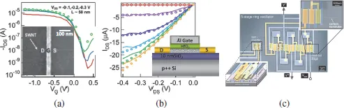
Table of contents
- Cover
- Halftitle
- Title
- Copyright
- Contents
- Chapter 1 Carbon Nanotube Flexible Electronics
- Chapter 2 Nanomaterial-Based Flexible Sensors
- Chapter 3 Graphene: From Synthesis to Applications in Flexible Electronics
- Chapter 4 Integrating Semiconductor Nanowires for High Performance Flexible Electronic Circuits
- Chapter 5 Graphene Devices for High-Frequency Electronics and THz Technology
- Chapter 6 Design of Nanostructures for Flexible Energy Conversion and Storage
- Chapter 7 Next Generation Flexible Solar Cells
- Chapter 8 Flexible Solar Cells
- Chapter 9 Recent Advances in Fiber Supercapacitors
- Chapter 10 Flexible Electronic Devices Based on Electrospun Micro-/Nanofibers
- Index
Frequently asked questions
- Essential is ideal for learners and professionals who enjoy exploring a wide range of subjects. Access the Essential Library with 800,000+ trusted titles and best-sellers across business, personal growth, and the humanities. Includes unlimited reading time and Standard Read Aloud voice.
- Complete: Perfect for advanced learners and researchers needing full, unrestricted access. Unlock 1.4M+ books across hundreds of subjects, including academic and specialized titles. The Complete Plan also includes advanced features like Premium Read Aloud and Research Assistant.
Please note we cannot support devices running on iOS 13 and Android 7 or earlier. Learn more about using the app