Theory and Methods of Photovoltaic Material Characterization
eBook - ePub

Theory and Methods of Photovoltaic Material Characterization

Optical and Electrical Measurement Techniques

  1. 328 pages
  2. English
  3. ePUB (mobile friendly)
  4. Available on iOS & Android
eBook - ePub

Theory and Methods of Photovoltaic Material Characterization

Optical and Electrical Measurement Techniques

Book details
Book preview
Table of contents
Citations

About This Book

This book provides an extensive review of the theory of transport and recombination properties in semiconductors. The emphasis is placed on electrical and optical techniques. There is a presentation of the latest experimental and theoretical techniques used to analyze minority-carrier lifetime. The relevant hardware and instrumentation are described. The newest techniques of lifetime mapping are presented. The issues are discussed relating to effects that mask carrier lifetime in certain device structures. The discrepancy between photoconductive and photoluminescence measurement results are analyzed.

Contents:

  • Semiconductor Fundamentals and Background
  • Optical Absorption and Radiative Recombination
  • Mobility and Defect Recombination
  • Carrier Diffusion and Confinement — Transient and Steady State Theory
  • Carrier Dynamics in Planar Device Structures
  • Transient Photoconductivity
  • Time-Resolved Photoluminescence: Techniques and Analysis
  • Auger Recombinationn
  • Trapping Spectroscopy
  • Steady State Techniques
  • Free Carrier Absorption
  • Recombination in Charge Separation Structures
  • Photon Recycling
  • Simultaneous and Comparative Measurements
  • Summary and Future Work


Readership: Science students and professionals in the field of physical chemistry and semiconductors, especially femtochemistry and those with interest in science. Photovoltaics;Optical and Electrical Measurement Techniques;Semiconductors;Carrier Transport;Recombination Lifetime;Carrier Lifetime;Minority Carrier Lifetime0 Key Features:

  • The topic is central and critical to photovoltaic device testing. Many researchers approach lifetime as a parameter that can be inferred indirectly from device performance or standard steady-state or transient measurements. This book updates the tools for comprehensive analysis of recombination phenomena and the influences of electrical injection levels, impurity-concentrations and spectra, surfaces and interfaces, and intrinsic materials properties

Frequently asked questions

Simply head over to the account section in settings and click on “Cancel Subscription” - it’s as simple as that. After you cancel, your membership will stay active for the remainder of the time you’ve paid for. Learn more here.
At the moment all of our mobile-responsive ePub books are available to download via the app. Most of our PDFs are also available to download and we're working on making the final remaining ones downloadable now. Learn more here.
Both plans give you full access to the library and all of Perlego’s features. The only differences are the price and subscription period: With the annual plan you’ll save around 30% compared to 12 months on the monthly plan.
We are an online textbook subscription service, where you can get access to an entire online library for less than the price of a single book per month. With over 1 million books across 1000+ topics, we’ve got you covered! Learn more here.
Look out for the read-aloud symbol on your next book to see if you can listen to it. The read-aloud tool reads text aloud for you, highlighting the text as it is being read. You can pause it, speed it up and slow it down. Learn more here.
Yes, you can access Theory and Methods of Photovoltaic Material Characterization by Richard K Ahrenkiel, S Phil Ahrenkiel in PDF and/or ePUB format, as well as other popular books in Physical Sciences & Physical & Theoretical Chemistry. We have over one million books available in our catalogue for you to explore.

Information

Publisher
WSPC
Year
2019
ISBN
9789813277144

CHAPTER 1

Semiconductor Fundamentals and Background

1.1.Tetrahedral Semiconductors

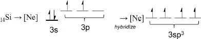
The material most widely associated with photovoltaics is silicon (Si), and its well-established properties are often the reference from which those of other PV materials are drawn. Silicon is a group-IV, tetravalent metalloid, inert, grey solid, with a high melting point (1400°C), a chemical analog to carbon. The four valence electrons of both Si and carbon (C) make these elements compatible with tetrahedral coordination. Building from the core of a neon (Ne) atom, a pair of spin-opposite electrons are first added to the 3s level, followed by two electrons in the 3p levels, which are spin aligned, according to Hund’s rule. The energy levels are shown in Fig. 1.1. Hybridization by linear combination of the 3s and 3p atomic orbitals can be used to form four molecular orbitals with minimal overlap. Whereas the hybridized levels have higher energy for isolated atoms, they result in an overall reduction in energy in the solid by forming tetrahedral bonds.
The molecular-orbital wave functions are constructed from linear combinations of these four, equally weighted orbitals:
images
images
Fig. 1.1.3sp3 hybridization.
images
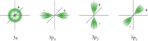
Fig. 1.2.Atomic orbitals that contribute to 3sp3 molecular orbitals.
images
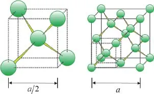
Fig. 1.3.The tetrahedron formed of nearest neighbors in Si can be inscribed within a cube of dimension a/2, where a is the cubic lattice parameter.
From the eight distinct possibilities generated by the various sign combinations, four can be selected with a tetrahedral arrangement. These functions are illustrated in Fig. 1.2.
Pure Si has the diamond crystal structure, most associated with carbon, which is comprised of two interpenetrating face-centered cubic lattices, both occupied by Si atoms, but separated by
images
the cube diagonal. The structures are shown in Fig. 1.3. Tetrahedral bonds associate each atom in either sublattice to the four nearest neighbors in the other sublattice. The tetrahedron formed among each atom and its four nearest neighbors can be inscribed within a cube of dimension a/2. Four such tetrahedra arranged with edges touching can be assembled into the full cubic unit cell.
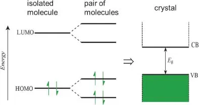
The electronic properties of crystals are influenced by the available states supported by the material and the distribution of electrons within these states. Continuous bands form that dictate the variation of energy with wave vector. The occupation of these bands depends on the numbers of electrons and temperature. Thus, the electrical-conduction properties of materials are closely linked to the band structure, carrier density, and temperature. Of utmost importance is the bandgap Eg — the energy between the highest occupied state and the lowest unoccupied state, which are derived from the highest-occupied and lowest-unoccupied molecular orbitals, [HOMO and LUMO, respectively] of isolated molecules. A schematic of these energy levels are shown in Fig. 1.4.
Semiconductor bandgaps are either direct or indirect, which refers to the alignment in crystal momentum space of the VB maximum and the CB minimum. For a direct-gap semiconductor, these are aligned in wave vector; for an indirect-gap semiconductor they are not aligned. The implication is that no change in crystal momentum is required for electronic transitions between the VB and CB. Thus, the transition may represent only a change in energy of an electron. That change in energy can occur by the absorption or emission of a photon which, as a massless particle, has negligible momentum. An indirect transition, on the other hand, requires concomitant momentum change, generally by the emission or absorption of a phonon.
images
Fig. 1.4.The semiconductor bandgap can be related back to the HOMO-LUMO energy difference of isolated molecules.
Bandgap is only one parameter describing the rather complex electronic structure of semiconductors. For example, the electronic bands of a three-dimensional crystal potential will not be spatially isotropic. The conductive properties of a semiconductor are dramatically influenced by doping, temperature, and illumination. These variations are exploited to enable control of electrical conduction for...

Table of contents

  1. Cover
  2. Halftitle
  3. Series Editors
  4. Title
  5. Copyright
  6. Contents
  7. Dedication
  8. Preface
  9. Acknowledgements
  10. 1. Semiconductor Fundamentals and Background
  11. 2. Optical Absorption and Radiative Recombination
  12. 3. Mobility and Defect Recombination
  13. 4. Carrier Diffusion and Confinement — Transient and Steady State Theory
  14. 5. Carrier Dynamics in Planar Device Structures
  15. 6. Transient Photoconductivity
  16. 7. Time-Resolved Photoluminescence: Techniques and Analysis
  17. 8. Auger Recombination
  18. 9. Trapping Spectroscopy
  19. 10. Steady State Techniques
  20. 11. Free Carrier Absorption
  21. 12. Recombination in Charge Separation Structures
  22. 13. Photon Recycling
  23. 14. Simultaneous and Comparative Measurements
  24. 15. Summary and Future Work
  25. Index