- English
- ePUB (mobile friendly)
- Available on iOS & Android
eBook - ePub
Power Management Techniques for Integrated Circuit Design
About this book
This book begins with the premise that energy demands are directing scientists towards ever-greener methods of power management, so highly integrated power control ICs (integrated chip/circuit) are increasingly in demand for further reducing power consumption.
- A timely and comprehensive reference guide for IC designers dealing with the increasingly widespread demand for integrated low power management
- Includes new topics such as LED lighting, fast transient response, DVS-tracking and design with advanced technology nodes
- Leading author (Chen) is an active and renowned contributor to the power management IC design field, and has extensive industry experience
- Accompanying website includes presentation files with book illustrations, lecture notes, simulation circuits, solution manuals, instructors' manuals, and program downloads
Tools to learn more effectively

Saving Books

Keyword Search

Annotating Text

Listen to it instead
Information
Edition
1 1
Introduction
1.1 Moore’s Law
Over the past few decades, the number of transistors per square inch on integrated circuits (ICs) has doubled every 18 months, which is the forecast of Moore’s law and is a continuing condition. However, a physical limitation appears when the transistor size shrinks to 28 nm. Several technology performance boosters, for example dual stress liner (DSL) technology, strained silicon techniques, and the stress memorization technique (SMT), are required to retain the performance of transistors. The industry has failed to keep to the trend predicted by Moore’s law. Figure 1.1 depicts how the rate of transistor size scaling has slowed down and is likely to break Moore’s law by the end of 2015.
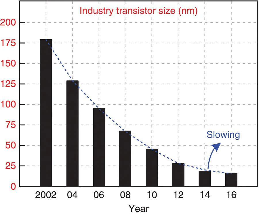
Figure 1.1 Transistor size scaling rate has slowed down
1.2 Technology Process Impact: Power Management IC from 0.5 micro-meter to 28 nano-meter
1.2.1 MOSFET Structure
The voltage stress issue of metal–oxide–semiconductor field-effect transistors (MOSFETs) in drivers and power MOSFETs needs careful consideration. The evolution of MOSFETs and their applications are based on different input supply voltage (Figure 1.2). In advanced processes (i.e., 40, 28, and 22 nm), core MOSFETs with characteristics of small silicon size and high speed are used in low-voltage applications. Moreover, conventional low-voltage MOSFETs are applied for low supply voltage conditions in normal processes, such as 22 nm, 0.18 μm, 0.25 μm, and 0.5 μm. Nevertheless, the drain-to-source voltage, VDS of low-voltage MOSFETs cannot tolerate a high voltage and punches, and will break the MOSFET when the input supply voltage increases. Therefore, double-diffused metal–oxide–semiconductors (DMOSs), vertical double-diffused metal–oxide–semiconductors (VDMOSs), and laterally diffused metal–oxide–semiconductors (LDMOSs) are applied to bear a high VDS. However, the gate-to-source voltage, VGS of such MOSFETs cannot endure a high voltage, which will also damage the MOSFET. A high-voltage metal–oxide–semiconductor (HVMOS) solves the problem here, because its structure can tolerate a high voltage of both VDS and VGS.
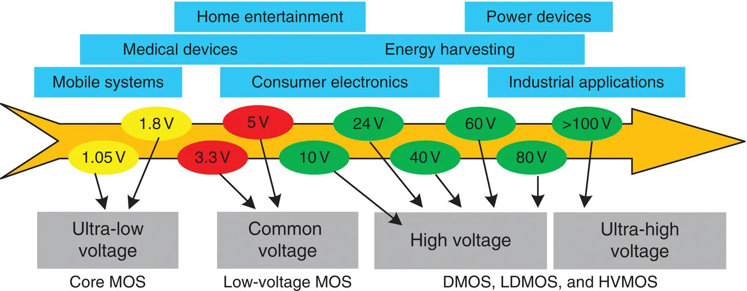
Figure 1.2 Evolution of MOSFETs and applications with different input supply voltages
The structures and characteristics of low-voltage MOSFETs, core MOSFETs, DMOSs, VDMOSs, LDMOSs, and HVMOSs are introduced in the following subsections, followed by a comparison of these MOSFETs.
1.2.1.1 Low-Voltage MOSFET
The structure of a typical n-channel low-voltage MOSFET is shown in Figure 1.3. Compared with LDMOSs and HVMOSs, the simple structure of a low-voltage MOSFET has the advantages of small silicon area and longest effective channel length (Leff), which is defined as the contact area between the p well and the gate in the n-channel low-voltage MOSFET. Moreover, a thin-gate oxide is designed to achieve the high-speed on-and-off switching of the MOSFET. However, this thin-gate oxide cannot bear th...
Table of contents
- Cover
- Title Page
- Table of Contents
- About the Author
- Preface
- Acknowledgments
- 1 Introduction
- 2 Design of Low Dropout (LDO) Regulators
- 3 Design of Switching Power Regulators
- 4 Ripple-Based Control Technique Part I
- 5 Ripple-Based Control Technique Part II
- 6 Single-Inductor Multiple-Output (SIMO) Converter
- 7 Switching-Based Battery Charger
- 8 Energy-Harvesting Systems
- Index
- End User License Agreement
Frequently asked questions
Yes, you can cancel anytime from the Subscription tab in your account settings on the Perlego website. Your subscription will stay active until the end of your current billing period. Learn how to cancel your subscription
No, books cannot be downloaded as external files, such as PDFs, for use outside of Perlego. However, you can download books within the Perlego app for offline reading on mobile or tablet. Learn how to download books offline
Perlego offers two plans: Essential and Complete
- Essential is ideal for learners and professionals who enjoy exploring a wide range of subjects. Access the Essential Library with 800,000+ trusted titles and best-sellers across business, personal growth, and the humanities. Includes unlimited reading time and Standard Read Aloud voice.
- Complete: Perfect for advanced learners and researchers needing full, unrestricted access. Unlock 1.4M+ books across hundreds of subjects, including academic and specialized titles. The Complete Plan also includes advanced features like Premium Read Aloud and Research Assistant.
We are an online textbook subscription service, where you can get access to an entire online library for less than the price of a single book per month. With over 1 million books across 990+ topics, we’ve got you covered! Learn about our mission
Look out for the read-aloud symbol on your next book to see if you can listen to it. The read-aloud tool reads text aloud for you, highlighting the text as it is being read. You can pause it, speed it up and slow it down. Learn more about Read Aloud
Yes! You can use the Perlego app on both iOS and Android devices to read anytime, anywhere — even offline. Perfect for commutes or when you’re on the go.
Please note we cannot support devices running on iOS 13 and Android 7 or earlier. Learn more about using the app
Please note we cannot support devices running on iOS 13 and Android 7 or earlier. Learn more about using the app
Yes, you can access Power Management Techniques for Integrated Circuit Design by Ke-Horng Chen in PDF and/or ePUB format, as well as other popular books in Technology & Engineering & Electrical Engineering & Telecommunications. We have over one million books available in our catalogue for you to explore.