Computer Science
Fetch Decode Execute Cycle
The Fetch-Decode-Execute cycle is the process by which a computer retrieves a program instruction from memory, decodes it, and then executes it. This cycle is repeated continuously, allowing the computer to carry out a series of instructions in order to perform a task.
Written by Perlego with AI-assistance
Related key terms
1 of 5
3 Key excerpts on "Fetch Decode Execute Cycle"
 eBook - ePub
Information Technology
An Introduction for Today's Digital World
- Richard Fox(Author)
- 2020(Publication Date)
- Chapman and Hall/CRC(Publisher)
own hardware. Fetching requires the PC and the L1 instruction cache where the PC is incremented before the end of the current cycle. Decoding uses the IR. Fetching operands uses the register file. Executing the instruction requires the ALU and if the instruction is a data movement operation (load or store from memory), the L1 data cache. Storing the result uses the register file. Two stages use the register file but accessing registers is the fastest part of this cycle, so we can accommodate all register accesses in one clock cycle.A pipeline of our five-stage fetch-execute cycle is shown in Figure 2.15 . The fetch stage uses the PC and instruction cache, with the PC being incremented after the instruction is fetched. The instruction, upon being fetched, moves into the IR, which is part of the decode stage. The control unit decodes the instruction in the IR to identify the operation and identify operand location. The operation is sent to the execute stage 2 cycles later to select the ALU circuit (for ALU operation) or data cache (for load or store operation) while the operand address information is used one and three stages later when selecting registers. In stage 3, any operands needed for the instruction are fetched from the register file. These values, along with the instruction from the decode stage, are moved into the execute stage. The execute stage, stage 4, receives the data and executes the instruction on that data. There are three general forms of execution: ALU operations, branches, and loads/stores. The figure shows the ALU. Branches modify the PC (not shown in the figure), so the PC could be changed both during the instruction fetch stage and the execute stage. Loads/stores use a separate data cache (not shown). In stage 5, any result from the ALU or loaded from the data cache is moved back into the register file.The key to understanding Figure 2.15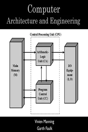 No longer available |Learn more
- (Author)
- 2014(Publication Date)
- College Publishing House(Publisher)
The program is represented by a series of numbers that are kept in some kind of computer memory. There are four steps that nearly all CPUs use in their operation: fetch , decode , execute , and writeback . The first step, fetch , involves retrieving an instruction (which is represented by a number or sequence of numbers) from program memory. The location in program memory is determined by a program counter (PC), which stores a number that identifies the current position in the program. In other words, the program counter keeps track of the CPU's place in the program. After an instruction is fetched, the PC is incremented by the length of the instruction word in terms of memory units. Often the instruction to be fetched must be retrieved from relatively slow memory, causing the CPU to stall while waiting for the instruction to be returned. This issue is largely addressed in modern processors by caches and pipeline architectures (see below). The instruction that the CPU fetches from memory is used to determine what the CPU is to do. In the decode step, the instruction is broken up into parts that have significance to other portions of the CPU. The way in which the numerical instruction value is interpreted is defined by the CPU's instruction set architecture ( ISA ). Often, one group of numbers in the instruction, called the opcode, indicates which operation to perform. The remaining parts of the number usually provide information required for that instruction, such as operands for an addition operation. Such operands may be given as a constant value (called an immediate value), or as a place to locate a value: a register or a memory address, as determined by some addressing mode. In older designs the portions of the CPU responsible for instruction decoding were unchangeable hardware devices. However, in more abstract and complicated CPUs and ISAs, a microprogram is often used to assist in translating instructions into various configuration signals for the CPU. No longer available |Learn more
- (Author)
- 2014(Publication Date)
- Learning Press(Publisher)
The program is represented by a series of numbers that are kept in some kind of computer memory. There are four steps that nearly all CPUs use in their operation: fetch , decode , execute , and writeback . The first step, fetch , involves retrieving an instruction (which is represented by a number or sequence of numbers) from program memory. The location in program memory is determined by a program counter (PC), which stores a number that identifies the current position in the program. In other words, the program counter keeps track of the CPU's place in the program. After an instruction is fetched, the PC is incremented by the length of the instruction word in terms of memory units. Often the instruction to be fetched must be retrieved from relatively slow memory, causing the CPU to stall while waiting for the instruction to be returned. This issue is largely addressed in modern processors by caches and pipeline architectures (see below). The instruction that the CPU fetches from memory is used to determine what the CPU is to do. In the decode step, the instruction is broken up into parts that have significance to other portions of the CPU. The way in which the numerical instruction value is interpreted is defined by the CPU's instruction set architecture ( ISA ). Often, one group of numbers in the instruction, called the opcode, indicates which operation to perform. The remaining parts of the number usually provide information required for that instruction, such as operands for an addition operation. Such operands may be given as a constant value (called an immediate value), or as a place to locate a value: a register or a memory address, as determined by some addressing mode. In older designs the portions of the CPU responsible for instruction decoding were unchangeable hardware devices. How-ever, in more abstract and complicated CPUs and ISAs, a microprogram is often used to assist in translating instructions into various configuration signals for the CPU. This
Index pages curate the most relevant extracts from our library of academic textbooks. They’ve been created using an in-house natural language model (NLM), each adding context and meaning to key research topics.