Physics
Ideal Op Amp
An ideal op amp is a theoretical electronic component with infinite input impedance, zero output impedance, infinite open-loop gain, and zero offset voltage. It is often used as a building block in electronic circuits for amplification, filtering, and signal processing due to its simplified and predictable behavior. However, real op amps have limitations that deviate from these ideal characteristics.
Written by Perlego with AI-assistance
Related key terms
1 of 5
12 Key excerpts on "Ideal Op Amp"
 eBook - PDF
Basic Electronics
Principles and Applications
- Chinmoy Saha, Arindam Halder, Debarati Ganguly(Authors)
- 2018(Publication Date)
- Cambridge University Press(Publisher)
OPAMP departs from the ideal behaviour in two ways. From a practical point of view, an ideal OPAMP is a device abstraction which acts as an ideal voltage-controlled voltage source. Referring to Figure 13.1, this implies that the device performs under the following assumptions: 1. No current flows into the input terminals of the device. This is equivalent to having an infinite input resistance R i = ∞. In practical terms, this implies that the amplifier device doesn’t draw power from the input signal source and isolate input signal source. 2. Have a zero output resistance ( R o = 0). This implies that the output voltage is independent of the load connected to the output. In addition, the ideal OPAMP model has infinite open-loop gain ( A → ∞). The ideal OPAMP model is shown schematically in Figure 13.4. Figure 13.4 Ideal OPAMP model TABLE 13.1 Summerizes the properties of an ideal OPAMP Table 13.1 Characteritics of an Ideal OPAMP PARAMETER NAME PARAMETER SYMBOL VALUE Input Impedance R i ∞ Output Impedance R o 0 Open-loop Gain A ∞ Input current I 1 and I 2 0 Input offset voltage v io 0 V i AV i I 2 I 1 + + + ---V 1 V 2 V O 624 Basic Electronics Even though practical OPAMP deviates from these ideal conditions, concepts of ideal OPAMP is very useful and are used extensively in circuit design and analysis. These assumptions make the analysis of circuit very simple and hence more insightful than the more rigorous actual model analysis. In the following sections, we will see how to use these rules. While using ideal OPAMP assumptions, we must remember that these assumption holds good, with in limit. For example, considering OPAMP as linear device, its input and output side voltage can be related as, v 0 = Av i i,e v v A i o = (13.1) Equation (13.1) implies that v i → 0 as A →∞. However, this does not mean that v 0 → 0. Rather for A → ∞, v i → 0 in such a way that their product Av i = v 0 ≠ 0. eBook - PDF
- Jiri Dostal(Author)
- 2013(Publication Date)
- Newnes(Publisher)
The only but principal limiting condition is that the feedback stability of the resulting closed loop must be preserved. 1.3 Ideal Operational Amplifier and Ideal Operational Circuit The seemingly absurd aim of every designer of operational amplifiers is to design an amplifier that is functionally invisible, in the sense that it does not affect the operational equation of the circuit. This abstraction is an ideal operational amplifier, a useful conception that allows rapid analysis of the nominal (i.e., desired) behavior of the operational circuit, or allows the design of the operational circuit on the basis of a given mathematical or even func-tional description, with results immediately and exactly applicable to an actual situation. Actual operational amplifiers, to a certain extent, approach their ideal. However, at a given state of technology, there is always a trade-off between quality, precision, and the higher complexity and price of the op-erational amplifier. • The ideal operational amplifier is an operational amplifier with zero dif-ferential input voltage and zero input currents for any output excitation and any common-mode input excitation, u d , I -, / + = 0 for any y 0 , / 0 , v cm . (1.3) • The ideal operational circuit is an operational circuit obtained by sub-stituting an ideal operational amplifier for the actual one. • The ideal operational equation is the operational equation of an ideal operational circuit. The value of these concepts will be appreciated in Chapter 4. As may be seen from Eq. (1.3), the ultimate quality of the operational amplifier depends upon the quality of its input side (upon the deviation of its input voltage and input currents from zero). To put this into the language of Chapter 2, an ideal operational amplifier has, at all frequencies, infinite open-loop gain, infinite common-mode rejec-tion ratio, infinite common-mode input impedances, and zero input error sources, as can also be deduced from Eq. eBook - PDF
Fundamentals of Electronics
Book 1 Electronic Devices and Circuit Applications
- Thomas F. Schubert, Ernest M. Kim(Authors)
- 2022(Publication Date)
- Springer(Publisher)
1 C H A P T E R 1 Operational Amplifiers and Applications e Operational Amplifier (commonly referred to as the OpAmp) is one of the primary active devices used to design low and intermediate frequency analog electronic circuitry: its importance is surpassed only by the transistor. OpAmps have gained wide acceptance as electronic building blocks that are useful, predictable, and economical. Understanding OpAmp operation is funda- mental to the study of electronics. e name, operational amplifier, is derived from the ease with which this fundamental building block can be configured, with the addition of minimal external circuitry, to perform a wide variety of linear and non-linear circuit functions. Originally implemented with vacuum tubes and now as small, transistorized integrated circuits, OpAmps can be found in applications such as: signal processors (filters, limiters, synthesizers, etc.), communication circuits (oscillators, modulators, demodulators, phase-locked loops, etc.), Analog/Digital converters (both A to D and D to A), and circuitry performing a variety of mathematical operations (multipliers, dividers, adders, etc.). e study of OpAmps as circuit building blocks is an excellent starting point in the study of electronics. e art of electronics circuit and system design and analysis is founded on circuit realizations created by interfacing building block elements that have specific terminal character- istics. OpAmps, with near-ideal behavior and electrically good interconnection properties, are relatively simple to describe as circuit building blocks. Circuit building blocks, such as the OpAmp, are primarily described by their terminal char- acteristics. Often this level of modeling complexity is sufficient and appropriately uncomplicated for electronic circuit design and analysis. However, it is often necessary to increase the complexity of the model to simplify the analysis and design procedures.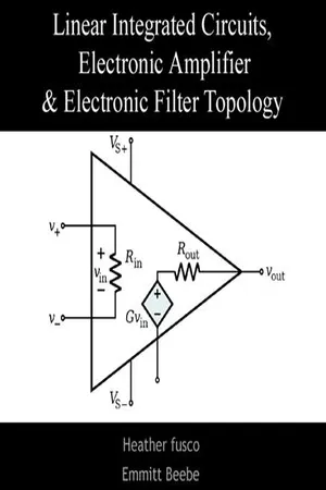 No longer available |Learn more
- (Author)
- 2014(Publication Date)
- College Publishing House(Publisher)
____________________ WORLD TECHNOLOGIES ____________________ • analog calculators • analog-to-digital converters • digital-to-analog converter • voltage clamps • oscillators and waveform generators Most single, dual and quad op-amps available have a standardized pin-out which permits one type to be substituted for another without wiring changes. A specific op-amp may be chosen for its open loop gain, bandwidth, noise performance, input impedance, power consumption, or a compromise between any of these factors. Limitations of real op-amps Real op-amps differ from the ideal model in various respects. IC op-amps as implemented in practice are moderately complex integrated circuits; the internal circuitry for the relatively simple 741 op-amp below, for example. DC imperfections Real operational amplifiers suffer from several non-ideal effects: Finite gain Open-loop gain is infinite in the ideal operational amplifier but finite in real operational amplifiers. Typical devices exhibit open-loop DC gain ranging from 100,000 to over 1 million. So long as the loop gain (i.e., the product of open-loop and feedback gains) is very large, the circuit gain will be determined entirely by the amount of negative feedback (i.e., it will be independent of open-loop gain). In cases where closed-loop gain must be very high, the feedback gain will be very low, and the low feedback gain causes low loop gain; in these cases, the operational amplifier will cease to behave ideally. Finite input impedances The differential input impedance of the operational amplifier is defined as the impedance between its two inputs; the common-mode input impedance is the impedance from each input to ground. MOSFET-input operational amplifiers often have protection circuits that effectively short circuit any input differences greater than a small threshold, so the input impedance can appear to be very low in some tests.
- J. David Irwin, David V. Kerns, Jr.(Authors)
- 2022(Publication Date)
- Wiley(Publisher)
CHAPTER 10 Operational Amplifiers and Applications LEARNING OBJECTIVES • To understand the characteristics of operational amplifiers and differential amplifiers • To understand the operation of the ideal op-amp model • To be able to recognize and analyze fundamental op-amp circuits • To understand the application of op-amps in the development of low-pass, high-pass, and bandpass filters • To be able to understand the use of op-amps to construct differentiator and integrator circuits • To understand multistage amplifier circuits • To be able to use op-amps in instrumentation and laboratory measurements and in industrial applications. INTRODUCTION The operational amplifier, or op amp as it is commonly known, is a fundamental component in analog electronic systems. Although it can be used in a variety of applications, it is widely used in instrumentation and measurement systems. An actual circuit diagram for a commercial op amp is the 741 Op Amp shown in Figure 10.1. Also shown in the figure are the pin connections for a dual in-line package, or DIP, which sup- ports its connection with other electronic components. Even a cursory examination of the circuit schematic for the op amp indicates that this is not a trivial network. It is typically constructed as an integrated circuit and may be purchased as a single device, in a DIP that contains several op amps or in a “surface mount” package. These elements are not only powerful devices in analog circuit design but are also inexpensive – less than a dollar for a chip in a package. Even after wading through the chapters in this book and developing a knowledge of transis- tors and their applications, the circuit diagram in Figure 10.1 may appear formidable. However, as sophisticated as it appears, it is really nothing more than a high-quality linear voltage ampli- fier. The details of how this circuit is designed are beyond the scope of this book, but follows basic principles described here. eBook - PDF
- B. Hart(Author)
- 1996(Publication Date)
- Butterworth-Heinemann(Publisher)
9 Operational amplifiers During World War II, engineers working on the design of military equipment used thermionic-tube amplifiers in circuits that simulated mathematical opera-tions, e.g, addition, subtraction and integration. Later, the term 'operational amplifier' came to be used in connection with such applications. Following the introduction of the (Fairchild) microelectronic amplifier type j.lA709, in 1965, the term 'operational amplifier' or one of its derivative forms, op-amp, OA (used henceforth), has been used to describe not a circuit function but the differential-input, high voltage-gain, direct-coupled Ie amplifier itself. Connected with other components in a feedback loop, the OA has given rise to a very large range of analogue circuits. Costing, now, little more than a few discrete passive components, e.g. resistors, the OA has largely revolutionized bread-and-butter analogue circuit design. It has also enabled engineers of other disciplines (e.g. mechanical, chemical) and scientists, generally, to design circuits having a precision and reproducibility that would previously have required the attention of an experienced electronics specialist. The aims of this chapter are: to introduce the OA and discuss an ideal model of it for use in first-order circuit analysis and design; to examine some basic circuit applications; and to define some of the most important parameters that char-acterize deficiencies, of practical OAs, and to consider the ways in which they restrict circuit operation. 9.1 IDEALIZED REPRESENTATION Figure 9.1(a) is a block schematic representation of an OA and, not being a wiring diagram, it does not show the presence of necessary power supplies, which are dealt with in Section 9.3. The two inputs Vp and VN and single output Va are referenced to a common line, i.e. chassis-earth. The letter A v inside the triangular symbol represents a voltage amplification function and does not have a sign associated with it. eBook - PDF
A Baker's Dozen
Real Analog Solutions for Digital Designers
- Bonnie Baker(Author)
- 2005(Publication Date)
- Newnes(Publisher)
C H A P T E R 5 Finding the Perfect Op Amp for Your Perfect Circuit 119 The operational amplifier’s operation and circuits are easy to find in the books in your local university library. The amplifier operation and circuit descriptions found in these reference books take you through computational algorithms that theoretically will provide the solutions to your analog amplifier design woes. If there were a perfect amplifier on the market today, the designs found in these books would indeed be easy to implement successfully. But there isn’t a perfect amplifier—yet. Throughout the history of analog system design, circuits have required special care in key areas in order to ensure success. As luck would have it, a little common sense and bench sense will pull you out of most of your amplifier, design disasters. In an ideal world, the perfect amplifier would look like the one described in Figure 5.1. (See Appendix C for definitions of specifications.) POWER SUPPLY • No Voltage Suppies Required • I SUPPLY = 0 Amps • Power Supply Rejection = ∞ (dB) OUTPUT • V OUT Swings Beyond Rails • I OUT = ∞ • Slew Rate = ∞ • Z OUT = 0 Ω SIGNAL TRANSFER • Open Loop Gain = ∞ (dB) • Bandwidth = 0 → ∞ • Zero Harmonic Distortion INPUT • Input Current (I B ) = 0 • Input Voltage (V IN ) → no limits • Zero Voltage and Current Noise • Zero Offset Voltage error • Common-Mode Rejection = ∞ (dB) $0.00 V DD V SS IN– IN+ OUT – + Figure 5.1: A perfect amplifier has an infinite input impedance, open-loop gain, power supply rejection ratio, common-mode rejection ratio, bandwidth, slew rate and output current. It also has zero offset voltage, input noise, output impedance, power dissipation and most importantly, zero cost. The input stage design of this perfect amplifier would use devices whose inputs (IN+ and IN–) extend all the way to the power supply rails. Some single-supply amplifiers are able to do this with some distortion, but the perfect amplifier would be distortion-free. No longer available |Learn more
- (Author)
- 2014(Publication Date)
- Research World(Publisher)
________________________ WORLD TECHNOLOGIES ________________________ Chapter 4 Operational Amplifier A Signetics μa741 operational amplifier, one of the most successful op -amps. An operational amplifier (op-amp) is a DC-coupled high-gain electronic voltage amplifier with a differential input and, usually, a single-ended output. An op-amp pro-duces an output voltage that is typically hundreds of thousands times larger than the voltage difference between its input terminals. ________________________ WORLD TECHNOLOGIES ________________________ Operational amplifiers are important building blocks for a wide range of electronic circuits. They had their origins in analog computers where they were used in many linear, non-linear and frequency-dependent circuits. Their popularity in circuit design largely stems from the fact that characteristics of the final elements (such as their gain) are set by external components with little dependence on temperature changes and manufacturing variations in the op-amp itself. Op-amps are among the most widely used electronic devices today, being used in a vast array of consumer, industrial, and scientific devices. Many standard IC op-amps cost only a few cents in moderate production volume; however some integrated or hybrid operational amplifiers with special performance specifications may cost over $100 US in small quantities. Op-amps may be packaged as components, or used as elements of more complex integrated circuits. The op-amp is one type of differential amplifier. Other types of differential amplifier include the fully differential amplifier (similar to the op-amp, but with two outputs), the instrumentation amplifier (usually built from three op-amps), the isolation amplifier (similar to the instrumentation amplifier, but with tolerance to common-mode voltages that would destroy an ordinary op-amp), and negative feedback amplifier (usually built from one or more op-amps and a resistive feedback network). No longer available |Learn more
- (Author)
- 2014(Publication Date)
- Academic Studio(Publisher)
In the first approximation op-amps can be used as if they were ideal differential gain blocks; at a later stage limits can be placed on the acceptable range of parameters for each op-amp. Circuit design follows the same lines for all electronic circuits. A specification is drawn up governing what the circuit is required to do, with allowable limits. For example, the gain may be required to be 100 times, with a tolerance of 5% but drift of less than 1% in a specified temperature range; the input impedance not less than one megohm; etc. A basic circuit is designed, often with the help of circuit modeling (on a computer). Specific commercially available op-amps and other components are then chosen that meet the design criteria within the specified tolerances at acceptable cost. If not all criteria can be met, the specification may need to be modified. A prototype is then built and tested; changes to meet or improve the specification, alter functionality, or reduce the cost, may be made. ____________________ WORLD TECHNOLOGIES ____________________ Basic single stage amplifiers Non-inverting amplifier An op-amp connected in the non-inverting amplifier configuration In a non-inverting amplifier, the output voltage changes in the same direction as the input voltage. The gain equation for the op-amp is: However, in this circuit V – is a function of V out because of the negative feedback through the R 1 R 2 network. R 1 and R 2 form a voltage divider, and as V – is a high-impedance input, it does not load it appreciably. Consequently: where Substituting this into the gain equation, we obtain: Solving for V out : If A OL is very large, this simplifies to . ____________________ WORLD TECHNOLOGIES ____________________ Inverting amplifier An op-amp connected in the inverting amplifier configuration In an inverting amplifier, the output voltage changes in an opposite direction to the input voltage. eBook - PDF
- James A. Svoboda, Richard C. Dorf(Authors)
- 2013(Publication Date)
- Wiley(Publisher)
CHAPTER 6 The Operational Amplifier I N T H I S C H A P T E R 6.1 Introduction 6.2 The Operational Amplifier 6.3 The Ideal Operational Amplifier 6.4 Nodal Analysis of Circuits Containing Ideal Operational Amplifiers 6.5 Design Using Operational Amplifiers 6.6 Operational Amplifier Circuits and Linear Algebraic Equations 6.7 Characteristics of Practical Operational Amplifiers 6.8 Analysis of Op Amp Circuits Using MATLAB 6.9 Using PSpice to Analyze Op Amp Circuits 6.10 How Can We Check . . . ? 6.11 DESIGN EXAMPLE— Transducer Interface Circuit 6.12 Summary Problems PSpice Problems Design Problems 6.1 I n t r o d u c t i o n This chapter introduces another circuit element, the operational amplifier, or op amp. We will learn how to analyze and design electric circuits that contain op amps. In particular, we will see that: Several models, of varying accuracy and complexity, are available for operational amplifiers. Simple models are easy to use. Accurate models are more complicated. The simplest model of the operational amplifier is the ideal operational amplifier. Circuits that contain ideal operational amplifiers are analyzed by writing and solving node equations. Operational amplifiers can be used to build circuits that perform mathematical operations. Many of these circuits are widely used and have been named. Figure 6.5-1 provides a catalog of some useful operational amplifier circuits. Practical operational amplifiers have properties that are not included in the ideal operational amplifier. These include the input offset voltage, bias current, dc gain, input resistance, and output resistance. More complicated models are needed to account for these properties. 6.2 T h e O p e r a t i o n a l A m p l i f i e r The operational amplifier is an electronic circuit element designed to be used with other circuit elements to perform a specified signal-processing operation. The mA741 operational amplifier is shown in Figure 6.2-1a. eBook - PDF
- Behzad Razavi(Author)
- 2021(Publication Date)
- Wiley(Publisher)
In this chapter, we study the operational amplifier as a black box, developing op-amp-based circuits that perform interesting and useful functions. The outline is shown below. 1 Vacuum tubes were amplifying devices consisting of a filament that released electrons, a plate that collected them, and another that controlled the flow—somewhat similar to MOSFETs. 355 356 Chapter 8 Operational Amplifier as a Black Box General Concepts • Op Amp Properties Linear Op Amp Circuits • Noninverting Amplifier • Inverting Amplifier • Integrator and Differentiator • Voltage Adder Nonlinear Op Amp Circuits • Precision Rectifier • Logarithmic Amplifier • Square Root Circuit Op Amp Nonidealities • DC Offsets • Input Bias Currents • Speed Limitations • Finite Input and Output Impedances 8.1 GENERAL CONSIDERATIONS The operational amplifier can be abstracted as a black box having two inputs and one output. 2 Shown in Fig. 8.1(a), the op amp symbol distinguishes between the two inputs by the plus and minus sign; V in1 and V in2 are called the “noninverting” and “inverting” inputs, respectively. We view the op amp as a circuit that amplifies the difference between the two inputs, arriving at the equivalent circuit depicted in Fig. 8.1(b). The voltage gain is denoted by A 0 : V out = A 0 (V in1 − V in2 ). (8.1) We call A 0 the “open-loop” gain. V V in1 in2 out V in1 in2 A 0 V V in1 V ( V in2 – out V (a) (b) ) Figure 8.1 (a) Op amp symbol, (b) equivalent circuit. It is instructive to plot V out as a function of one input while the other remains at zero. With V in2 = 0, we have V out = A 0 V in1 , obtaining the behavior shown in Fig. 8.2(a). The positive slope (gain) is consistent with the label “noninverting” given to V in1 . On the other hand, if V in1 = 0, V out = −A 0 V in2 [Fig. 8.2(b)], revealing a negative slope and hence an “inverting” behavior. eBook - PDF
- Richard C. Dorf, James A. Svoboda(Authors)
- 2020(Publication Date)
- Wiley(Publisher)
6.7-1. In other words, the finite gain model of the operational amplifier reverts to the ideal operational amplifier as the gain becomes infinite. The gain for practical op amps ranges from 100,000 to 10 7 . E X A M P L E 6 . 7 - 2 Finite Gain In Figure 6.7-3, a voltage follower is used as a buffer amplifier. Analysis based on the ideal operational amplifier shows that the gain of the buffer amplifier is v o v s 1 What effects will the input resistance, output resistance, and finite voltage gain of a practical operational amplifier have on the performance of this circuit? To answer this question, replace the operational amplifier by the operational amplifier model that accounts for finite voltage gain. This gives the circuit shown in Figure 6.7-3b. + – v o + – + – v s v 2 v 1 v o v 2 v 1 v o i 1 i 2 R 1 R 1 R L + – v o v s R i R L – + (a) (b) i o i L + – R o A(v 2 – v 1 ) FIGURE 6.7-3 (a) A voltage follower used as a buffer amplifier and (b) an equivalent circuit with the operational amplifier model that accounts for finite voltage gain. Characteristics of Practical Operational Amplifiers 241 Solution To be specific, suppose R 1 1 kV; R L 10 kV; and the parameters of the practical operational amplifier are R i 100 kV, R o 100V, and A 10 5 V/V. Suppose that v o 10 V. We can find the current i L in the output resistor as i L v o R L 10 10 4 10 3 A Apply KCL at the top node of R L to get i 1 i o i L 0 It will turn out that i 1 will be much smaller than both i o and i L .
Index pages curate the most relevant extracts from our library of academic textbooks. They’ve been created using an in-house natural language model (NLM), each adding context and meaning to key research topics.